Sunday, June 11, 2023

PCIe Deep Dive, Part 2: Stack and Efficiency

Before getting too caught up in the inner workings of PCIe, it's probably worth taking a look at the high-level architecture - how it's used in a system and what the PCIe controller stack looks like. PCIe is fundamentally a bi-directional memory bus extension: it allows the host to access memory on a device and a device to access memory on the host.

When a PCIe link is established between the host and a device, the host assigns address space(s) that it can use to access device memory. Optionally, it can also grant permission for the device to access portions of host system memory. In that way, the host and device memory buses are effectively connected. Each PCIe link is a point-to-point connection, but they can be combined with switches into a fabric with many devices (endpoints).

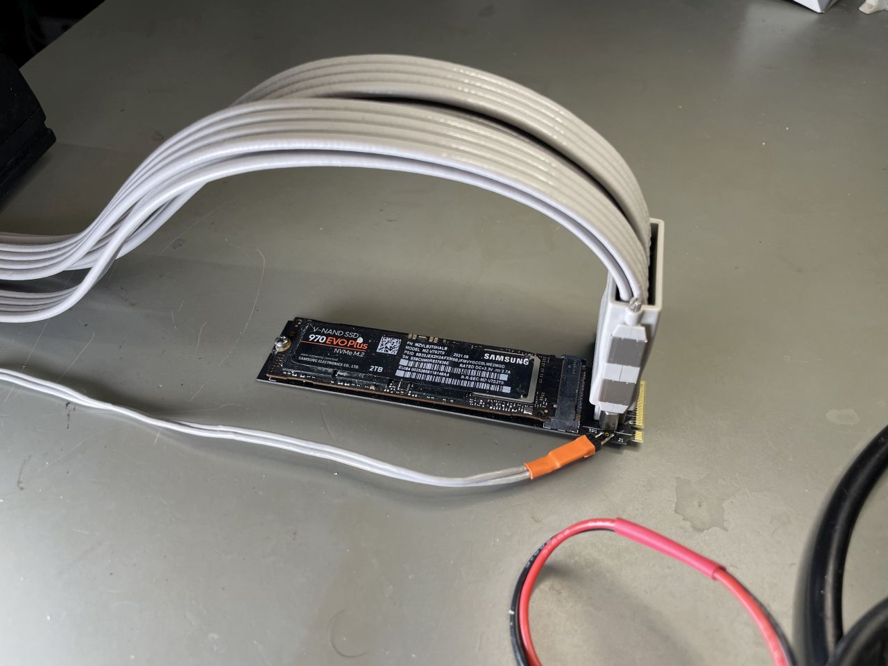
Different types of devices utilize the memory bus bridging capability of PCIe in different ways. For example, an NVMe storage device exposes only a small amount of device memory (the NVMe Controller Registers) that the host uses to configure the device and inform it when new commands have been submitted. All actual data transfer is done by the storage device reading from or writing to host memory. In this way, the NVMe storage device acts as a DMA controller between host memory and non-volatile storage.

NVMe storage device usage of PCIe link (completion steps omitted).

One might ask why the memory buses can't just be directly connected. For one, a native memory interface such as AXI is very wide: it might have 64-256b of data, 32-64b of address, and a bunch of control signals. This works fine inside a chip, but going from chip-to-chip, board-to-board, or across a cable, it's too many signals. The PCIe Controller encapsulates the data, address, and control signals from the memory bus into packets that can be sent across a fast serial link over a small number of differential pairs. This standard interface also allows bridging memory buses with different native interfaces, speeds, and latencies.

With that context in mind, we can look at the PCIe Controller stack, and what role each layer plays in bridging memory transactions between the host and device as efficiently and reliably as possible. The PCIe specification defines three layers: the Transaction Layer (TXL), the Data Link Layer (DLL), and the Physical Layer (PHY). These layers each have a transmit and a receive side. From the point of view of the host, the stack looks like this:

Memory transactions from the host to the device are packaged by the TXL into a Transaction Layer Packet (TLP) with a header containing the address and other control information. The DLL prepends a framing token (STP) and appends a CRC to the TLP to create a Link Packet. This is then split into lanes and serialized by the PHY. The process happens in reverse for memory transactions from device to host, to go from serialized Link Packets back to host memory transactions.

In practice, many architectures (including Ultrascale+) break the PHY into two parts: an upper Media Access Control (MAC) layer and a lower layer still called the PHY. These are connected by the standard PHY Interface for PCI Express (PIPE), published by Intel. It's also useful to add an explicit AXI-PCIe bridge layer above the TXL when the native memory bus is AXI, as it is in the Ultrascale+ architecture. This would be an example of what some references call the Application Layer. Expanded this way, the stack looks like this:

Different Xilinx IPs cover different layers of the stack, as shown above. PG239 (PCI Express PHY) is a low-level (PIPE down) PCIe PHY wrapper for the GTH/GTY serial transceivers. PG213 (UltraScale+ Devices Integrated Block for PCI Express) covers the PCIE4 hardware block that includes the TXL, DLL, and MAC layers, and interfaces to the PHY via PIPE. And PG194 (AXI Bridge for PCI Express Gen3 Subsystem) includes the AXI-PCIe bridge layer on top of the PCIE4 hardware block and PHY. (For Ultrascale+, this is technically implemented as a configuration of PG195, but the relevant documentation is still in PG194.)

All of these Xilinx IPs are included in Vivado at no additional cost, but not every device has the PCIE4 block(s) needed to instantiate PG213 or PG194/PG195. For the Zynq Ultrascale+ line, the product tables show how many PCIe lanes are supported by integrated PCIE4 blocks for each device. In general, the larger and more expensive chips have more available PCIe hardware. But there are exceptions like the ZU6xx, ZU9xx, and ZU15xx, which have none. These can still instantiate PG239, but require a PCIe soft IP to implement the rest of the stack.

Each layer communicates with the next through a data bus that's sized to match the speed of the link. The example above is for a Gen3 x4 link, which supports 32Gb/s of serial data in each direction. In the Ultrascale+ implementation, the 250MHz clock for the 128b internal datapath is derived from the PCIe reference clock, so all layer logic is synchronous with the PHY. This seems like a perfectly-balanced data pipeline, with 32Gb/s of data coming in and going out in each direction. But in practice, overheads limit the maximum link efficiency.

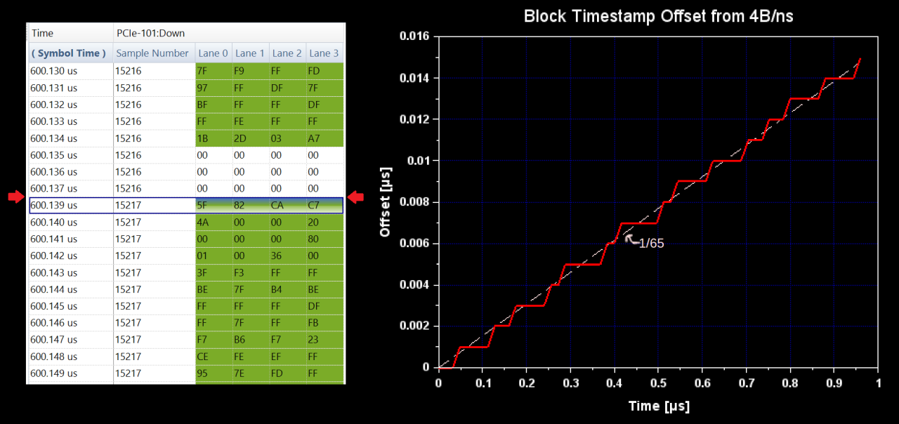
First, PCIe Gen3 uses 128b/130b encoding: for each 128b serial data payload on each lane, a 2b sync header is prepended to create a 130b block. The sync bits tell the receiver whether the block is data or an Ordered Set (control sequence). In order to make room for the sync bits, PIPE requires one invalid data clock cycle in every 65-clock period.

The period for skipping data on the 250MHz side of the PHY is 260ns, while the period for a 130b serial output block is only 16.25ns, so the PHY must implement buffering and a SERDES gearbox to make this work. The effect of the sync bits can be seen in the protocol analyzer raw data, where there are occasionally 1ns gaps in the timestamp. (The full serial data rate including sync bits would be exactly 4B/ns.) These leap-nanoseconds add up to an overall efficiency of 98.5% (64/65), as can be seen by plotting the starting timestamp of each block.

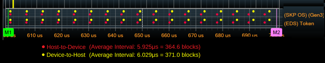
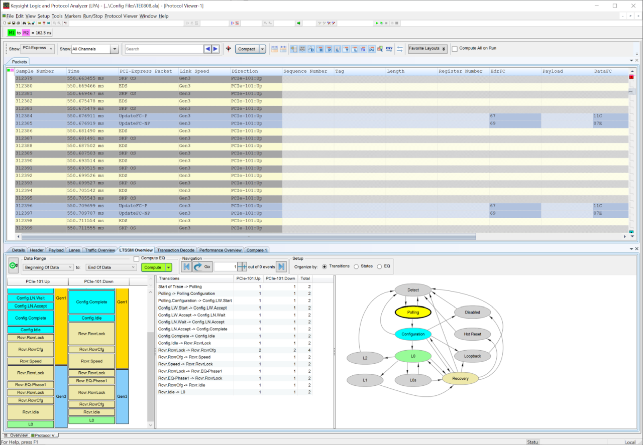
Next, transmitters are required to periodically stop transmitting data and send a SKP Ordered Set (SKP OS), which is used to compensate for clock drift. This should happen every 370-375 blocks, and the SKP OS takes one block to transmit. Stopping the data stream also requires sending an EDS token, which may require one additional block depending on packet alignment. But even in a worst-case scenario this still represents about 99.5% (368/370) efficiency.

We can see the EDS tokens and SKP OS at regular intervals in both directions on the protocol analyzer. Interestingly, the average interval in the Host-to-Device direction is on the short side (365 blocks). Maybe it's not accounting for the 64/65 PIPE TxDataValid efficiency described above. The interval is controlled by the MAC layer, which is in PG213 in this case, so I don't think it's something that can be adjusted. The Device-to-Host direction is spot-on in this case, with a 371-block interval.

DLLs also exchange Data Link Layer Packets (DLLPs) for Ack/Nak and flow control of TLPs. These packets are short (6B), but they must be transmitted with enough regularity to meet latency requirements and ensure receiver buffers don't overflow. There's no simple rule for when these are transmitted, only a set of constraints based on the link operating conditions. To get a feel for the typical link efficiency impact of DLLP traffic, we can look at a 100μs section of bulk data transfer and add up the combined contribution of all DLLPs:

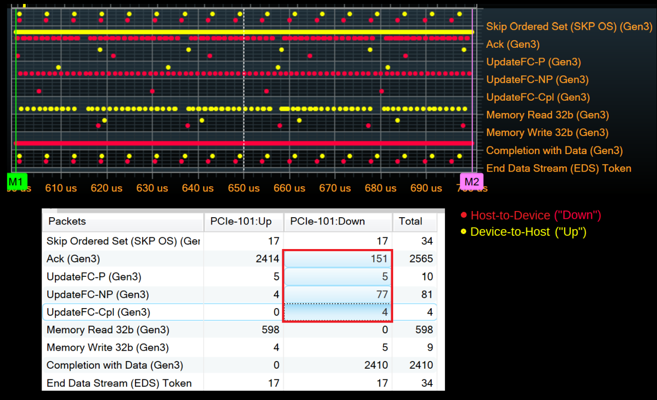
In total, there were 237 DLLPs transmitted in the Host-to-Device direction. Since the packets must be lane-0-aligned on an x4 link, they actually occupy 8B each. This is 1896B of overhead for nearly 400000B of data, again around 99.5% efficiency. This example is mostly unidirectional data transfer from host to device, though. If the device was also sending data to the host, there would be far more Acks going in the Host-to-Device direction. If the Ack count were similar to that of the Device-to-Host direction in this example, the efficiency would drop to around 95%.

Lastly, the biggest overhead is usually for TLP packetization. The TLP header is either 12B or 16B. The DLL adds a 4B framing token (STP) and a 4B Link CRC (LCRC). The payload size can be as high as 4096B, although it's limited to 1024B in the Ultrascale+ implementation (PG213). It's also common for devices to limit the max payload size to 128B, 256B, or 512B, depending on the capability of their PCIe Controller. This gives a range of 84.2% (128/150) to 98.1% (1024/1044) for packetization efficiency with optimally-sized transfers on Ultrascale+ hardware.

In the example capture, data is transferred from host to device in 128B-payload TLPs:

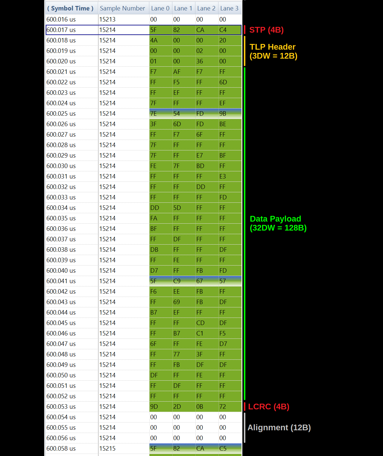
The packet has 20B of overhead for 128B of data, which would be an 86.5% efficiency. However, the host controller also inserts 12B of logical idle (zeros) to align the next STP token to the start of a block. This isn't required by the PCIe protocol, but may be inherent in the implementation of the controller. For this payload size, it drops the efficiency to 80% (128/160). 

That packetization efficiency dominates the overall link efficiency, which hovers between 75% and 80% during periods of stable data transfer:

In this case, increasing the max payload size would have the most positive impact on throughput. PG213 can go up to 1024B, but the device controller may be the limiting factor.

In PCIe 6.0, a big change will be introduced that removes sync bits and consolidates DLLPs, framing tokens, and the LCRC into a fixed 20B overhead in each 256B unit (called a FLIT, for Flow Control unIT). This implies a fixed 92.2% efficiency for everything other than the SKP OS and TLP header overhead, and also a fixed latency for Ack/Nak and flow control, a nice simplification.

But for now we're still in the realm of PCIe Gen3, where we can expect an overall link efficiency in the 75-95% range, depending on the variety of factors described above as well as details of the controller implementations.

The packetization and flow control functions described above are the domain of the Transaction Layer and Data Link Layer, but there are also some really interesting functions of the MAC and PHY layers that facilitate reliable serial data transfer across the physical link. These will have to be topics for one or more future posts, though.

Sunday, May 7, 2023

PCIe Deep Dive, Part 1: Tool Hunt

Over the past few years, I've been developing and improving very fast standalone NVMe-based storage capability for the Zynq Ultrascale+ architecture, to keep up with the absurd speeds of modern SSDs. (Drives like the Seagate Firecuda 530 and Sabrent Rocket 4 Plus-G can now hit 3GB/s+ sustained TLC write speeds, with much higher pSLC cache peaks.) But my knowledge pretty much ended at the interface to the Xilinx DMA/Bridge Subsystem for PCI Express (PG194/PG195). In the usual fashion, I'm now going to dive deeper to explore in more detail how the AXI-PCIe bridge works, and what the PCIe stack actually looks like.

Something I found interesting about PCIe in general is that there seems to be a pretty large barrier built up around the black box. Even just finding learning resources is much harder than it should be. The best I found was PCI Express Technology 3.0 and some accompanying material by MindShare, but even that seems like a prose wrapper on top of the specification. There isn't anything that I would consider a beginner's guide, like you might find for USB or Ethernet.

[Edit by Future Shane] There is a very good series of four articles from Simon Southwell starting here that offers a thorough introduction to PCIe. Definitely check it out if you're going to be exploring PCIe.

For physical tools, the situation is even more bleak. The speeds in PCIe Gen3 (8GT/s) put it in the range where an oscilloscope that can actually measure the signal will cost more than a car. But for all but the lowest-level hardware debugging, a digital capture would suffice, and that's where a protocol analyzer would be nice. Unfortunately, there is no Wireshark equivalent for PCIe; protocol analyzers for it are dedicated hardware that only a few companies develop, and they are priced astronomically.

That is...unless you scout them on eBay for a year.

Biggest "that escalated quickly" of my test equipment stack (ref. PicoScopes below table).

This is a used U4301B that I got in what has to be my second-best eBay score of all time, for less than it would have cost me to rent one for a month. There are only ever a handful of them up for auction at any given time, and the market is so small that the price is basically random, so if you're actually looking for one I can only wish you luck. This one goes up to Gen3 x8, which is fine for my purposes. If you only need Gen1/2 capability, the situation is much better.

[Edit by Future Shane] There is one listed on eBay for a good price right now if anyone else is looking for one. (I'll remove this note after it's no longer available.)

The U4301B is actually just the instrument in the bottom slot of the M9505A AXIe Chassis. This is meant to connect to a PCIe slot on a host machine using an iPass cable and interface card. Newer versions of the chassis controller have a laptop-friendly Thunderbolt connection instead. I "upgraded" mine using an eGPU enclosure, the smaller black box sitting on top.

I said that the U4301B was my second-best eBay score of all time, and that's because the number one is the U4322A probe that I got to go with it, from a different auction. The protocol analyzer is useless without a probe or interposer, and those are even harder to find used. I have never seen a U4322A on eBay before or since the one I got, and all other online listings for them are dead-ends. So the fact that I got one for what might as well be free compared to the new cost is just plain luck.

It was, however, a lot broken...

The probe has two rows of spring-loaded contacts that are meant to touch down on test pads for the PCIe signals. Unfortunately, mine was missing several pins and many others were bent or broken. It had been treated like a scrap cable, rather than a delicate probe. No problem, though, I can just replace the spring pins with some equivalent Mill-Max parts...

...oh, well shit.

This was one of the most ridiculous things I have ever seen under the microscope. Each spring pin has a surface-mount resistor soldered into its tip, and encased in epoxy. What the multi-GHz fuck is going on with these? Well, I suspect they each make up part of a passive probe, also called a Low-Z or Z0 probe. This video explains the concept in detail; it's forming a resistive divider with the 50Ω termination. But it must have extremely low capacitance on the input side of the resistor, hence the resistors embedded in the tips. The good news is that there are no amplifiers in the probe head, so there's not much else that can be broken.

There's no replacement for these pins, so the ones that were missing or broken were a lost cause. But luckily there were enough intact ones to make a full bidirectional x4 link, which is all I really needed. They weren't all in the right locations, so I had to carefully rearrange them with a soldering iron, taking care to use as little solder as possible while still making a strong connection. After making the x4 link, there are only a couple of spare pins remaining, so I need to be very careful with this probe.

Actually the U4322A was not my first choice; what I really wanted was a U4328A M.2 interposer, which taps off the signals at an M.2 connector bridge. But I can convert my basically free U4322A into that using a basically free circuit board. This board just has the test pad footprint for the U4322A in between a short M.2 extension. I carefully mounted the U4322A to the board with standoffs and don't really intend to ever take it off again.

Somewhat to my surprise, this collection of parts actually does work. I was worried that there would be some license nonsense involved, but the instrument license seems to go with the instrument. The host software doesn't require a separate license and worked right away, even through my weird Thunderbolt eGPU enclosure hack. And that's really where the value is. It wouldn't be hard to make an in-system PIPE traffic logger on a Zynq Ultrascale+, and I might do that anyway, but parsing and visualizing the data in a convenient way takes a lot of effort. With the LPA Software, you just get nice graph and packet views straight away:

This all seems like a lot of effort for probing an interface that's now at least two generations old. All this equipment is outdated and could for sure be replaced with a single-board interposer based on a Zynq Ultrascale+. All it needs is two GTH quads, a bunch of RAM, and a high-speed interface to the outside world. But I don't think Keysight or Teledyne LeCroy are interested in that - Gen5 is where the money is. Interestingly, though, the new Keysight Gen5 analyzer is a single-board interposer.

But for now I have Gen3 protocol analysis capability, which is good enough for my purposes. I've used it a bunch in the past few months to explore the different layers of the PCIe stack and components within. There are some really interesting parts that I may cover in future posts. But I'll probably start with an overview of the whole stack, and where the available Xilinx IPs fit into it, since even that is a little confusing at first. There are hard and soft (i.e. HDL) components to it, and not every device has an out-of-the-box solution for making the whole stack. That's enough material for an entire post though, so I'll end this one here.

Saturday, October 9, 2021

Zynq Ultrascale+ Bare Metal NVMe: 2GB/s with FatFs + exFAT

This is a quick follow-up to my original post on speed testing bare metal NVMe with the Zynq Ultrascale+ AXI-PCIe bridge. There, I demonstrated a lightweight NVMe driver running natively on one Cortex-A53 core of the ZU+ PS that could comfortably achieve >1GB/s write speeds to a suitable M.2 NVMe SSD, such as the Samsung 970 Evo Plus. That's without any hardware acceleration: the NVMe queues are maintained in external DDR4 RAM attached to the PS, by software running on the A53.

I was actually able to get to much higher write speeds, over 2.5GB/s, writing directly to the SSD (no file system) with block sizes of 64KiB or larger. But this only lasts as long as the SLC cache: Modern consumer SSDs use either TLC or QLC NAND flash, which stores three or four bits per cell. But it's slower to write than single-bit SLC, so drives allocate some of their free space as an SLC buffer to achieve higher peak write speeds. Once the SLC cache runs out, the drive drops down to a lower sustained write speed.

It's not easy to find good benchmarks for sustained sequential writing. The best I've seen are from Tom's Hardware and AnandTech, but only as curated data sets in specific reviews, not as a global data set. For example, this Tom's Hardware review of the Sabrent Rocket 4 Plus 4TB has good sustained sequential write data for competing drives. And, this AnandTech review of the Samsung 980 Pro has some more good data for fast drives under the Cache Size Effects test. My own testing with some of these drives, using ZU+ bare metal NVMe, has largely aligned with these benchmarks.

The unfortunate trend is that, while peak write speeds have increased dramatically in the last few years, sustained sequential write speeds may have actually gotten worse. This trend can be seen globally as well as within specific lines. (It might even be true within different date codes of the same drive.) Take for example the Samsung 970 Pro, an MLC (two bit per cell) drive released in 2018 that had no SLC cache but could write its full capacity (1TB) MLC at over 2.5GB/s. Its successor, the 980 Pro, has much higher peak SLC cache write speeds, nearing 5GB/s with PCIe Gen4, but dips down to below 1.5GB/s at some points after the SLC cache runs out.

Things get more complicated when considering the allocation state of the SSD. The sustained write benchmarks are usually taken after the entire SSD has been deallocated, via a secure erase or whole-drive TRIM. This restores the SLC cache and resets garbage collection to some initial state. If instead the drive is left "full" and old blocks are overwritten, the SLC cache is not recovered. However, this may also result in faster and more steady sustained sequential writing, as it prevents the undershoot that happens when the SLC cache runs out and must be unloaded into TLC.

So in certain conditions and with the right SSD, it's just possible to get to sustained sequential write speeds of 2GB/s with raw disk access. But, what about with a file system? I originally tested FatFs with the drive formatted as FAT32, reasoning (incorrectly) that an older file system would be simpler and have less overhead. But as it turns out, exFAT is a much better choice for fast sustained sequential writing.

The most important difference is how FAT32 and exFAT check for and update cluster allocation. Clusters are the unit of memory allocated for file storage - all files take up an integer number of clusters on the disk. The clusters don't have to be sequential, though, so the File Allocation Table (FAT) contains chained lists of clusters representing a file. For sequentially-written files, this list is contiguous. But the FAT allows for clusters to be chained together in any order for non-contiguous files. Each 32b entry in the FAT is just a pointer to the next cluster in the file.

FAT32 cluster allocation entirely based on 32b FAT entries.

In FAT32, the cluster entries are mandatory and a sequential write must check and update them as it progresses. This means that for every cluster written (64KiB in maxed-out FAT32), 32b of read and write overhead is added. In FatFs, this gets buffered until a full LBA (512B) of FAT update is ready, but when this happens there's a big penalty for stopping the flow of sequential writing to check and update the FAT.

In exFAT, the cluster entries in the FAT are optional. Cluster allocation is handled by a bitmap, with one bit representing each cluster (0 = free, 1 = allocated). For a sequential file, this is all that's needed. Only non-contiguous files need to use the 32b cluster entries to create a chain in the FAT. As a result, sequential writing overhead is greatly reduced, since the allocation updates happen 32x less frequently.

exFAT cluster allocation using bitmap only for sequential files.

The cluster size in exFAT is also not limited to 64KiB. Using larger clusters further reduces the allocation update frequency, at the expense of more dead space between files. If the plan is to write multi-GB files anyway, having 1MiB clusters really isn't a problem. And speaking of multi-GB files, exFAT doesn't have the 4GiB file size limit that FAT32 has, so the file creation overhead can also be reduced. This does put more data "at risk" if a power failure occurs before the file is closed. (Most of the data would probably still be in flash, but it would need to be recovered manually.)

All together, these features reduce the overhead of exFAT to be almost negligible:

With 1MiB clusters and 16GiB files, it's possible to get ~2GB/s of sustained sequential file writing onto a 980 Pro for its entire 2TB capacity. I think this is probably the fastest implementation of FatFs in existence right now. The data block size still needs to be at least 64KiB, to keep the driver overhead low. But if a reasonable amount of streaming data can be buffered in RAM, this isn't too much of a constraint. And of course you do have to keep the SSD cool.

I've updated the bare metal NVMe test project to Vivado/Vitis 2021.1 here. It would still require some effort to port to a different board, and I still make no claims about the suitability of this driver for any real purposes. But if you need to write massive amounts of data and don't want to mess around in Linux (or want to try something similar in Linux user space...) it might be a good reference.

Sunday, September 12, 2021

TinyCross: New UI and Front Wheel Traction Control

 In the last post, I finally did some actual data logging with TinyCross set up in 4WD, 80A peak per motor, which is the rated current. Based on tinyKart, I know they can handle a a bit more for short durations, maybe even up to 120A. But the data logs (and many instances of having rocks flung into my face) demonstrate that the front wheels reach their traction limit somewhere around 60A on asphalt.

The behavior of front wheel slip on a go-kart is something new to me. In a straight line, the initiation of the slip and the acceleration of the wheel actually isn't the biggest problem. It's when the wheel regains traction and slows down that bad things happen. The restored grip combines with the energy being dumped from the wheel's moment of inertia to generate a quick pulse of torque on that side, which creates a lot of torque steer.

To deal with this, I wanted to implement some form of traction control, at least for the front wheels, so that I could get the most torque out of them as possible without the steering disturbances and rock shooting. But first, I needed a way to easily configure both the motor currents and the traction control settings without having to drag around my laptop everywhere. So, I finally built out the steering wheel UI to include a bunch of settings:

Sorry for the exposure; it's the only way to capture the full OLED refresh period.

Anyone familiar with the MōVI Controller might recognize the OLED display. I chose this for daylight visibility and responsiveness (~50Hz update rate). The menu interface is essentially the same as the one I built the day before NAB 2014... The left knob scrolls through the menu. The right knob adjust settings and, by clicking or holding, performs actions.

In the four corners are three motor parameters for the corresponding motors: S for Status, which shows error codes. F for Forward peak current, and R for Reverse (braking, or actually reversing) peak current. Setting both to zero masks out the CAN command from that motor, triggering a timeout that turns off the gate drivers entirely. A click and hold on S triggers an encoder recalibration for that motor.

In the second column from the left, the first three settings relate to data logging: LS for Logger Status, FN for File Number (click to start a new file), and LT for Logger Time, the time in [ms] for a single row of the data log to be written. Then, there are two parameters for tuning traction control: TT for Traction Threshold, and TG for Traction Gain, which I will explain shortly.

The reason I wanted to be able to adjust peak currents from the steering wheel is because I agree with this early Tesla blog post: "...it's much safer to avoid wheelspin altogether than react to it." If I know the surface supports front wheel current around 60A, there's not much point in setting it higher than that. But, I want to be able to set it higher for testing, or adjust it for different surfaces.

As for the traction control itself, there are a lot of corner cases to think about in 4WD, but the main problem I'm trying to solve is front wheel slip. If I assume the rear wheels are not slipping, then I can use their average speed as a reference. From there, it's easy to see if a front wheels is running faster than that reference, and reduce the current to that motor if so. This only needs two settings: a Traction Threshold (TT) that sets how much wheel slip is allowed, and a Traction Gain (TG) that sets how much to reduce the current per unit slip above the threshold. The Traction Threshold prevents overactuation in normal conditions and allows for speed differential due to turning radius.

But what happens if a rear wheel does slip? Well, then the front wheel might slip too. At that point, I'm probably in some kind of a four wheel sideways drift anyway, so alternate control laws are going to apply. Being able to trigger some rear wheel slip with the throttle is part of the fun, too, so having complete 4WD traction control isn't something I necessarily need to solve.

With the new UI setup and the simple front wheel traction control in place, it was time to do some tuning...

...or not.

At first, everything seemed to be going okay. I did a couple of runs at 60A front current and 80A rear current and the traction control seemed to be working as intended. But then during light regenerative braking at around 30mph, I heard the all-too-familiar sound of a FET popping, followed by some more bad noises and smells from the front drive. Upon inspection, only two FETs actually died, but they also took out many of the power traces, meaning this board was trash.

So what happened? Well, unfortunately, the data log was not very helpful in this case. It did show the speed (30mph) and current command (around -10A), but nothing out of the ordinary up until the point of failure. There is only one data point showing a Q-Axis current of 286A on the front left motor, followed by an undervoltage fault, which might have been the battery sagging or the power input traces getting blown up. So whatever happened, happened quick.

It's been a while since I've actually destroyed a motor controller, so I was a little disappointed. But after some thought, I didn't think this was due to the new traction control stuff. That's only applied during acceleration, and this failure definitely happened under braking. I think it's more likely that the front left motor just lost sync and the back EMF at 30mph was high enough to do damage. Up until now, I have only had a relatively slow overcurrent limit of 160A (or more) for 10ms. These FETs have a pretty insane Safe Operating Area (SOA), but that limit does leave room for exceeding it with currents above 400A:

This system could easily generate a 400A transient if a motor loses sync at 30mph. And the motor position and speed data does cut out at the same data point as the failure. But that's not enough to determine cause and effect. So for now I can only make changes that might help and hope for the best. I added in several more stages of faster overcurrent protection, up to 300A for a single ADC/PWM cycle (42.7μs). These overlap enough to cover the entire R_DS(on)-limited boundary of the SOA (up to the pulse rating of 1450A for 100μs!).

A faster overcurrent trip doesn't help with whatever caused the motor to lose sync in the first place (if that is what happened). I have seen at least a couple previous instances where the encoders, which supply emulated Hall effect sensor signals, have behaved as if they were completely reset. Even though I only use the buffered and optically isolated virtual Hall effect sensor signals for commutation, I was still reading the SPI data anyway. Maybe a SPI read got corrupted by noise and turned into a write that either reconfigured or entirely reset the encoder mid-run? To protect against this, I now disabled the SPI transactions entirely other than during initialization and calibration.

So with these changes and my last and only spare drive, I went back out for another try. This time, I ran into no motor drive issues and was actually able to test and tune the front wheel traction control as I originally intended. The difference is immediately obvious while driving and in the data. First, a test at 80A front, 90A rear, with no traction control:

Front wheel traction control off.

As before, the front right wheel starts slipping at about 60A and spins up to 2-3x the actual ground speed. The front right always seems to lose grip first, a mystery to solve another day. When I let off the throttle and it regains traction, the torque pulse creates substantial torque steer, jerking the steering wheel almost 20º to the left, which I then have to counteract immediately to stay on course. Overall, it's impossible to sustain peak acceleration for more than a second or so before having to deal with the wheel spin and torque steer.

And now with the same currents, but front wheel traction control on:

Front wheel traction control on.

The front right (FR) current now averages a bit below 60A and its speed is held to just a small margin above the actual ground speed. It's never able to build up momentum and then "catch", inducing torque steer. This allows continuous acceleration up to and past 30mph. The front left (FL) also starts to slip in the 20-30mph range, but the traction control catches it too. The overall result is a much more controllable launch and far fewer rocks being thrown up by the front wheels.

After finding traction control settings that I liked, I switched back to current settings that more closely match the actual traction limits: 60A front and 100A rear. This still gives a reasonable 0.45g launch, but with less likelihood of triggering the traction control on asphalt. I'd like to push to >0.5g, to match tinyKart's most extreme configuration, but that'll either require 120A on the rear or changing the gear ratio a bit. At 60A / 100A, the front motors still share enough of the load that the rear motors stay at healthy temperature after some acceleration runs:

Rear motors are doing most of the work, but...

...they are at a reasonable temperature.

And finally I did some less structured testing by just driving through the gravel corner in my parking lot and intentionally adding throttle to induce slip. It behaves pretty well, slipping and oversteering about the right amount to be controllable but still fun:


I think at this point most of the handling bottlenecks are back on the mechanical side. There's a small amount of backlash in the steering column that definitely exaggerates the residual torque steer, especially at high speeds. It's almost all coming from the U-joint, which I may try to shim or replace with one with tighter tolerances. Other than that, I need to do some suspension geometry tweaking to improve handling of lateral transients. Speaking of which, here's one last data capture. See if you can figure out what's going on here...

Mystery data log.

Sunday, August 15, 2021

TinyCross: 4WD 80A Data Logging

It's been a long time since I did a proper test drive with TinyCross, although I've taken it out just for fun a few times. Since I completed the weight/width reduction pass last week, I wanted to get it out again and do some proper data logging in 4WD, with the peak current set to 80A for all four motors. This is still below the ultimate target of 100-120A (for short bursts), but plenty for parking lot testing.

Really enjoying the extra 2" of clearance - I can get through most of the "doors" in my building now.

I had to inflate the tires, but amazingly the air shocks don't seem to have leaked at all after a year of neglect. And they still do a pretty impressive job of soaking up the awful topography of my parking lot.

I wanted to do some more thorough data logging in 4WD to characterize some of the issues I've felt while just driving around for fun. The steering wheel PCB collects data from the front and rear motor drives over CAN, appends some of its own data, and writes the whole thing to a microSD card. When I first set this up, I just had it overwrite the existing data log every power cycle. But in the couple of years since I set that up, I've had to master FatFs. So setting it up to create new files on the fly without messing up any of the real-time stuff was an easy upgrade.

Here's what a 4x80A launch looks like:

4x80A launch (attempt).

The main problem is pretty obvious from the data: the front wheels just don't have enough weight on them to support 80A. If there's even a little bit of a loose surface, one or both front wheels will lose grip. Excessive wheel slip is inefficient, so the peak acceleration isn't as high as it could be if all four wheels hugged their grip limit. But front wheel slip is especially bad because it results in massive torque steer. (I actually used this to make remote-control TinyCross.) It also has a habit of throwing rocks up into the driver's face.

I've even debated whether the front wheel drive on TinyCross is worth the extra weight and complexity. tinyKart handled pretty well with RWD only: I could put in a controlled amount of oversteer with the throttle. In fact, I got a chance to test out how TinyCross feels with RWD only when I had - let's call it an 80/20 failure - on the front right upright:

Always check your T-nuts! The only real casualty was the encoder wire.

Although I was able to fix the mechanicals with the single hex driver I always bring with me, a few crimps pulled out of the encoder wire and I didn't have the tools to fix it. I could probably add a failover to sensorless operation for individual motors, but I'm not sure how well it'd work on the front motors, again because of torque steer. (Both fronts would have to agree to not produce torque until the flux estimator converges on the sensorless motor.) For now, I just removed power from the front drive.

In terms of handling, RWD works fine. But the launch is a mere 0.25g at 2x80A. There's no slip, and even if there was, it wouldn't matter as much on the rear since it doesn't induce torque steer.

2x80A launch.

Even at 120A, this would only be about a 0.4g launch. tinyKart, in its last and somewhat scary configuration, was hitting about 0.5-0.6g. Part of this is down to gearing: TinyCross, with 12.5" wheel, has to be geared for higher speeds. I could always ditch the front motors and switch to 80mm motors with more torque on the rear. But I think that goes against the spirit of TinyCross. Having full independent suspension and 4WD has always been the point.

So I think I'll finally have to dive in to writing some simple traction/launch control software. Just looking at the 4x80A launch data, it's easy to pick out the wheel that's slipping and imagine that the software could just fold back the current command to that wheel as its speed starts to diverge from the other three. But there are so many logical knots on the path to generalizing that to 4WD, where any subset of the four wheels could be slipping, that it makes my brain hurt to even think about.

There are some amazing technical blog posts from the early days of Tesla (back when it was more of an engineering project than a consumer electronics device) where they talk about how it took months to go from a controller with excellent high-bandwidth torque control to functioning traction control, and even then a lot of it was subjective. One observation I really liked:

This type of feedforward traction control can be hugely beneficial; for instance, it's much safer to avoid wheelspin altogether than react to it.

This was regarding a lateral G observer that was fed into the friction model that the traction control software used to help limit motor torque to what it thought the tires could reasonably handle. This way, wheel slip might be limited to cases where there truly is a sudden drop in friction at one wheel. I think that should be the goal for this as well. I might even be able to just do slip detection on the front wheels. It'll be an interesting experiment, at least.

Saturday, August 7, 2021

TinyCross Weight and Width Reduction Pass

It's summer, which means it's time to work on go-karts. This round, it's a modification to TinyCross that I've been wanting to make ever since I first got it together about two years ago. The main issue is that I designed it around stock rear 12.5" scooter wheels. These are almost symmetric and have threading on both sides of the hub that are meant for mounting the drive sprocket and brake disk. But - and this is maybe my favorite bit of packaging on this project - I've got the brake and drive sprocket both mounted to the inboard side, with the brake caliper sitting right in the middle of the belt:

The brake and drive sprocket are both mounted to the inboard side of the wheel, making the outboard side of the hub dead weight.

This makes the extended length of the outboard side of the hub useless. But, I left it as stock for simplicity. I figured if I ever needed to replace the wheels, it would be easier to drop in a new stock 12.5" wheel. But, this drives the overall width of the kart up to about 35" for no good reason:

The total width, about 35", is driven in part by the symmetric 12.5" wheel hubs.

It's also unnecessary weight, especially factoring in the beefier 5"x5/8" hex standoffs I used to close the structural loop around each wheel. I figured I could eliminate 2" off the total width and about 1lb off the total weight if I just bit the bullet and re-machined the 12.5" wheel hubs. It still wouldn't fit through a 32" door frame, but it would be easier to wiggle through indoor spaces and fit in my car. It also would just look a lot nicer.

One of the reasons I put off this modification for so long is because I thought it would involve disassembling the entire wheel module, but it turns out that it's just barely possible to remove the wheel without removing the motor. I can take off the brake caliper and slip the belt off the pulley to give it just enough slack to pull the wheel off the spindle shaft. I don't remember intentionally designing it this way, but let's pretend I did. It'll be good for fixing flats, too. 

The next obstacle to overcome was removing the outboard bearings. I didn't have a bearing puller on-hand, but I discovered that an 80/20 T-Nut (which I obviously have hundreds of...) is just about exactly the right size to push on the outer race of these bearings. So I came up with this improvised tool:

Improvised bearing pusher.

The tool is built inside the hub by slipping the 80/20 T-Nut through the bearing, flipping it horizontal, then dropping in the hex standoff from the other side. After fastening it together with a 1/4-20, it's ready for the press. Luckily, I didn't Loctite these bearings in, so they pressed out pretty easily.

Pressing out the bearings using the makeshift pusher.

The 12.5" wheels don't fit on my mini lathe, but they do just barely fit on my mini-mill. I knew this ahead of time, so I bought a 22mm end mill specifically for cutting the new bearing pocket. (One of the nice features of this mini-mill is its use of a regular R8 spindle, so it's possible to get large tools for it.) I did have to get a little creative with fixturing. The brake disk is bolted down to a piece of 80/20, which is clamped in the mill. But, to make things stiff enough, I also had to ground the rim itself directly to the bed with some long clamping screws.

Clamping situation: not great, not terrible.

Pretty sure this mill was never meant to hold a tool this big.

I decided to extend the bearing pocket by 1.000" first, before machining down the hub by 1.000". I'm not sure if this was the best order of operations, but it all went pretty smoothly. Here's 7:45 of relaxing slow-motion bearing pocket cutting, captured at 4K 420fps with my Wave:

These hubs are cast aluminum, so it wasn't surprising to find that there were some voids in the newly-machined faces. They're nothing that I think would affect the structural integrity, but it's an interesting consequence of the manufacturing process.

Casting voids exposed by re-machining the hubs.

One of the downsides of doing this operation on the mill is that I didn't have a choice of machining the new bearing pocket to an interference fit. But I was pleased to see that, with all the extra effort put into stiffening the fixture, it was still a nice slip fit. I can always add Loctite later if needed.

After re-machining, the bearings are now a nice slip fit.

That just leaves the 7075 spindle shafts, which also needed to be shortened by 1.000". Cutting off the extra length and extending the outboard mounting hole was a quick task for the mini-lathe. Then, it just needed to be re-tapped.

Shortening the 7075 spindle shafts...

...and re-tapping.

Finally, I put everything back together, substituting much lighter 4"x1/2" hex standoffs to span the gap at the top of each wheel module. The total process took only about two hours per wheel, including disassembly and reassembly. So something I have put off for two years was really only one day of work...typical. Anyway, the final result is a kart that's now 2" narrower and about 1lb lighter.

The pile at the front is roughly the weight saved. (5"x5/8" standoffs were replaced by 4"x1/2", but an equivalent amount of weight was taken out of each hub.)

I have a few more tasks I want to do on this kart. It still needs to be fully weather-proofed. I have a plan for enclosing the motor drives, but need to figure out something for the steering wheel PCB. I may redesign that board from scratch since I don't think I'll ever get to using the battery balancing circuit on it. It can be much smaller and simpler without that. Lastly, there's always motor drive stuff to fiddle with to squeeze out more torque and/or speed.

For now, though, I'm glad it's a little lighter and a lot narrower. It'll make deploy that much easier, which ultimately means more actual testing and use.

Saturday, April 18, 2020

Full-Speed CMV12000 Subsampled Readout: 1440fps 1080p

Now that I've got a continuous multi-Gpx/s image capture pipeline running, it's time to rearrange some things to break the 1000fps barrier:


For this clip I'm using the CMV12000's X/Y subsampling mode to trade resolution for frame rate, hitting 1440fps at 2048x1088. The overall pixel rate is a little lower than in 4K (3.2Gpx/s vs. 3.8Gpx/s), so it's feasible to send this through the same Zynq Ultrascale+ capture pipeline, with some modifications, to record continuously to an NVMe SSD. With ~4:1 wavelet compression, this writes about 1GB/s to the drive, up to 1000s (16.7min) for a 1TB drive. That would be 16.7 hours of playback at 24fps, though. I figured 30 seconds real-time and 30 minutes of playback was enough water droplet footage for now.

CMV12000 Subsampling

In a previous post, I covered the pipeline architecture for continuously recording 400fps 4K video from a CMV12000 image sensor to an NVMe SSD. That was a 4096x2304 (16:9) frame, slightly larger than 4K UHD. The sensor's native resolution is 4096x3072 (4:3), which it can read in at 300fps. By reading in fewer rows, the maximum frame rate is increased. Going wider than 16:9 would allow frame rates higher than 400fps, but since the sensor always reads in full 4096px-wide rows, the speed gain is only linear.

To go much faster, it's necessary to read in fewer columns as well. Not all sensors can do this; reading whole rows may be baked into the hardware architecture. The CMV12000 doesn't support arbitrary readout width, but it does support 2x subsampling. In this mode, every other four-pixel square (Bayer group) is skipped in both the X and Y directions. The remaining squares are transmitted on the LVDS channels using an alternate packing:

CMV12000 subsampled readout (color, X-flipped).
Each of the 64 LVDS channels alternates between two rows, with the lower 32 channels handling two even (G1/R1) rows and the upper 32 channels handling two odd (B1/G2) rows. This alternate data packing allows the subsampled image, with 1/4 as many total pixels, to be read out nearly 4x faster. There is a small amount of extra overhead time that makes the actual gain not quite 4x.

Subsampling drops the resolution from 4K to 2K but preserves the crop factor of the sensor, since the full width and height are still used. This is preferable to cropping a 2048px-wide image out of the middle. It doesn't give any increase in sensitivity though; to do that would require binning (averaging the larger 4x4 squares to generate the final 2x2). The CMV12000 does support binning, but the overhead is so bad that you might as well read out the 4K image and do it in post (assuming you have the data storage bandwidth, which I certainly do). So to go ~4x faster, I will need ~4x more light.

Light sensitivity of subsampling vs. binning.
Before worrying about a shortage of photons, though, I first need to deal with a shortage of programmable logic. To fit everything on the XCZU4, my main bottlenecks are BRAMs and LUTs. I managed to add the decoder for HDMI output with no increase in either by sacrificing the third wavelet stage. But I've known for a long time that the day would come when I would need to add 128 more Stage 1 horizontal cores to handle the subsampled inputs.

It might seem odd that more cores are needed to process a smaller image. Even at the higher frame rate, the pixel input rate is lower than in 4K. Surely the existing horizontal cores could time-multiplex to handle the data? But, the wavelet cores must operate on groups of adjacent pixels. In this case, adjacency describes the nearest horizontal pixels of the same color, since applying a difference operation to pixels of different colors would not have the desired result. And whatever the color, pixels from another row are not horizontally adjacent. Since each LVDS channel now services two color fields and two rows, it must feed four independent wavelet cores.

In 2K mode, each LVDS channel feeds four independent Stage 1 horizontal cores.
So, the total number of Stage 1 horizontal cores doubles from 128 to 256. This jump has been on my mind since the early stages of the design, and I tried to optimize the horizontal cores as much as possible. A big part of this was reducing the operating pixel width from 16-bit to 12-bit, which brought the per-core LUT count down from 107 to 83. As this is the first stage of the pipeline, it's easy to verify that it won't saturate on 10-bit inputs. The horizontal cores operate in-line with the input using only distributed memory, so no additonal BRAMs are required. But there's now way around the additional 10,000 or so LUTs, and that will bring me right up to the limits of this chip.

Since I knew there would be very few LUTs remaining for switching modes, I originally thought the 4K and 2K modes might have to exist as entirely separate PL configurations, their bitstreams loaded on as-needed by software. I've seen other cameras do this; it looks like a software reset when changing capture formats. And while it only takes a few seconds, I really dislike the workflow and the idea of maintaining two configurations.

So, I spent some time looking at the actual differences between modes at all stages of the pipeline and decided that I could and should build the switch. I had this mode change in mind early in the design, so I tried to minimize the number of touch points required in each of the modules to switch between 4K and 2K. Even so, there are a number of small changes needed in the Wavelet, Encoder, and HDMI modules. They are collectively driven by a master switch in each module's AXI slave registers. I'll go through them in pipeline order below.

Wavelet Stage 4K/2K Switch

First, no actual switching is required to distribute the inputs to the Stage 1 horizontal cores; each channel always connects to the same four cores. Instead, the cores are gated by a master pixel counter based on their color and, when in 2K mode, also their row. The 2K mode switch turns on this extra enable gate and offsets the counter that handles first/last row states by one bit, to account for the half-width rows. Miraculously, this did not add any LUTs to the horizontal cores. I assume the extra logic just got merged into existing smaller LUTs...I'll take it.

The most complicated part of the switch happens next, at the interface between the Stage 1 horizontal and vertical cores. Instead of distributing outputs from four adjacent horizontal cores into a single row of a vertical core BRAM, the 2K interface distributes outputs from eight horizontal cores into two rows of a vertical core BRAM. Since the rows are half as wide, this takes the same number of pixel clock cycles (128). So, as will be the case at many points in the pipeline, this just boils down to rearranging the bits of the BRAM write address:

Aspect ratio change and read/write addressing of the Stage 1 vertical core BRAMs in 4K vs. 2K mode.
Conceptually, the aspect ratio of the vertical core BRAM changes from 8 rows of 256px to 16 rows of 128px. The figure above shows where writes and reads occur in the BRAM at a given relative pixel count. Reads occur on half-counts since the Stage 1 vertical DWT operates at double px_clk frequency. The read address generator is also modified by the switch to account for the new aspect ratio. Only the eight most recent rows are actively written or read, so in 2K mode the BRAM is twice as big as it needs to be. The latency of the vertical core is also halved, since it's determined by the number of rows required to complete the vertical DWT operation. This will come into play later.

The Stage 1 vertical core buffers the alternating-row 2K mode inputs into a single-row format that's compatible with the rest of the pipeline, so changes after this point are relatively minor. Each Stage 1 vertical core feeds its output row to a Stage 2 horizontal core. The only modification required there is to offset the counter that handles first/last row states by one bit, to account for the half-width rows. Then, the Stage 2 vertical core just needs some more BRAM address rearrangement:

Aspect ratio change and read/write addressing of the Stage 2 vertical core BRAMs in 4K vs. 2K mode.
Like the Stage 1 vertical core BRAM, the aspect ratio is changed from 8 rows of 256px to 16 rows of 128px. But since the first stage already rearranged things into single rows, the write addressing here is more straighforward: In both 4K and 2K mode, only a single row is filled at a time (by two adjacent Stage 2 horizontal cores). The row width is halved, but there's no write interleaving between the two rows. Ultimately, this is just a different arrangement of the write address bits. The read address generator is similarly modified to grab the right data for the Stage 2 vertical DWT. As with the Stage 1 vertical core, the BRAM is twice as big as it needs to be, and the latency is halved.

Encoder 4K/2K Switch

The compression stage doesn't care about the aspect ratio change, since the only context it uses for variable-length encoding is an immediate group of four pixels. However, it does need to know the adjusted latency of both wavelet stages, since the first pixel to be encoded will arrive sooner in 2K mode. For that, I just made all the latency offsets software-defined, through the encoder's AXI slave registers. And that should be the only change required here...

Except things are never that easy. I noticed after plugging in the expected latency values in 2K mode, two of the four color fields (R1 and G2) were actually dropping one pixel per row. It took a while to isolate this to the encoder, and then even more staring at this module to figure out what the problem was. Since the only change I made was to the latency offsets, I figured there had to be some fundamental difference between how the local pixel counter (px_count_e) drives the encoder states during row transitions with different offsets, and there was:

Encoder gating in 4K mode, showing the difference between sequential and combinational px_count_e_updated.
The above shows px_count_e at the first row overhead time (ROT) in 4K mode. It's negative since pixels haven't made it to the encoder yet, but the same behavior happens at all subsequent row transitions. During ROT, the sensor is not sending pixel data and all the pixel counters (including px_count_e) hold their previous values. A signal called px_count_e_updated is cleared, which gates the encoder from sending pixels to RAM (via an intermediate shift register called e_buffer). This signal was previously sequential, which would add one clock cycle delay between the ROT and when the encoder is gated. It should have been combinational, to line up correctly with the ROT.

But the write to e_buffer also only takes place every other group of four pixel clocks, for reasons discussed here. In 4K mode, the ROT happens to fall in a period where writes don't occur anyway. The sequential vs. combinational difference didn't matter to the final e_buffer_wr_en signal. But in 2K mode, the new latency offsets just happen to put the ROT one cycle before the start of a four-cycle write sequence, where the difference does matter:

Encoder gating in @K mode, showing the difference between sequential and combinational px_count_e_updated.
After switching over to combinational logic for px_count_e_updated, the missing pixel returned, and things were almost happy again. It turns out there was a similar issue at the quantizer and encoder modules themselves, before the write to e_buffer. This was simply due to them not being enable-gated at all, though. (Again, it must have been working thanks to lucky latency offsets in 4K mode.) Gating each with the same combinational px_count_e_updated signal worked fine.

HDMI 4K/2K Switch

But wait, isn't the HDMI output always 1080p? While that is true, it doesn't mean there's nothing to be done here. In 4K mode, only the Stage 2 wavelet compression is decoded, leaving a 2K preview image (really, four color fields that are each 1024px wide) to be output via HDMI. This greatly reduces the size of the HDMI module, since it only has to decode four of the sixteen codestreams and do one stage of inverse DWT. However, getting to the same preview size in 2K mode would mean complete decoding, require all sixteen codestreams and two wavelet stages. I simply don't have room to do that, so I'm going to cheat.

The first step is to change how the viewport is mapped to a pixel count. To achieve arbitrary scaling of the preview image, I first normalize the viewport to 16-bit, i.e. top-left (0, 0) to bottom-right (65535, 65535). The x and y components, vxNorm and vyNorm, are shifted around to create the pixel counters that drives the output pipeline. When switching from 4K to 2K, each component gets right-shifted by one and the split between x and y moves over by one bit in the final counter:
Mapping between 16-bit (vxNorm, vyNorm) coordinates and opx_count in 4K vs. 2K mode.
This remapping means that the entire output pipeline operates at half resolution in 2K mode. The preview will actually just be scaled up from the four LL1 color fields, which are each 512px wide. There will still be bilinear interpolation to help smooth out the result, but it will be blurrier than the 1080p preview in 4K mode. But again there isn't really an alternative, at least not with the resources I have left on this chip.

The output pixel counter (opx_count) drives all parts of the decoding process, starting with a RAM reading FIFO through the HDMI module's AXI master. No changes are required there or in the decoder itself, other than modifying the latency offsets accordingly. These have always been software-defined, so I just added the expected values for 2K mode and they worked without any hassle. (There was no equivalent sequential vs. computational bug, thankfully.)

After this, the modifications to the Stage 2 inverse vertical wavelet cores are pretty simple and almost the same as in the forward direction. Each color field's IV2 core uses a single URAM for row storage. In 2K mode, the aspect ratio is changed from 16 rows of 1024px to 32 rows of 512px, by rearranging read and write address bits:

Aspect ratio change and read/write addressing of the Stage 2 inverse vertical core URAMs in 4K vs. 2K mode.
Unlike the forward direction, the Stage 2 inverse horizontal wavelet cores also use URAMs for row storage and these likewise need address bit rearrangement to change aspect ratios for 2K mode:

Aspect ratio change and read/write addressing of the Stage 2 inverse horizontal core URAMs in 4K vs. 2K mode.
And finally, the bilinear interpolation module needs to be adjusted to automatically scale up the preview image by 2x, so it can fill the viewport using the 512px-wide color field LL1 outputs. This can be done quickly by passing the shifted vxNorm and vyNorm values to the module, although this isn't quite correct, as will be discussed below. It's good enough for now, though.

Debayering

Applying an ordinary debayering algorithm, whatever it is, to the 2K subsampled raw data doesn't really work. This is because the physical spacing between pixels is no longer symmetric. For example, a red pixel is closer to its green and blue neighbors to the left and below than to the right and above. A proper bilinear interpolation needs to take this asymmetry into account, by modifying the location of pixel centers for each color field accordingly. More advanced algorithms are still built on the assumption of symmetric neighbors, so they'd all need modification to some degree.

Asymmetric neighboring pixels in subsampled mode can be handled by modifying interpolation pixel centers (left) or with an intermediate supersampling step (right).
Alternatively, the subsampled data can be supersampled by 2x to estimate the missing pixels (G2' and G1' in the image above) and then run through the ordinary debayer algorithm in 4K. The final output can then be scaled back to 2K to reflect the true information content of the data. This path takes longer for what may be an equivalent result for simpler debayer algorithms, but it might have advantages for more complex algorithms. All this will probably be obsoleted by neural networks that upscale 240p images to 16K in a few year anyway, so I'm not going to worry about it.

It is important to adapt the debayer algorithm for the subsampled pixel locations somehow, though, or there will be significant artifacts. The following comparison shows three different algorithms, nearest-neighbor, bilinear, and a Microsoft 5x5 interpolator that I like. For each, a reference 4K capture and 4K debayer is compared to a 2K subsampled capture with an unmodified 2K debayer and a 2K subsampled capture with a supersampled 4K debayer.

Comparison of three different interpolation algorithms with 4K capture/debayer, 2K subsampled capture with unmodified 2K debayer, and 2K subsampled capture with supersampled 4K debayer.
None of these simple algorithms can do much to recover resolution - for that I defer to the AI supersampling state of the art - but using an unmodified 2K debayer on subsampled raw data creates significant color checkerboarding artifacts on edges. Supersampling the data by 2x and running a simple 4K debayer at least bypasses the problem of neighboring pixel asymmetry.

Resource Utilization

Squeezing in the 4K/2K switch was beyond what I'd hoped to fit on the XCZU4, but it just barely works. The switch itself really only adds LUTs where BRAM/URAM address bits are remapped or where pixel counts are shifted to account for the aspect ratio change. The main addition is the 128 new Stage 1 horizontal wavelet cores, which really push the resource utilization to the limits.

The XCZU4 with everything crammed in.
At this point I'm at 77143 LUTs (87.82%), 93883 FFs (53.44%), 118 BRAMs (92.20%), 14 URAMs (29.17%) and 146 DSPs (20.05%). But, since most of my cores are running at px_clk (60MHz) or HDMI clock (74.25MHz) frequency, the timing constraints are not too difficult to meet. The exception seems to be things that interact with the 250MHz AXI clock, including the encoder and decoder BRAM FIFOs. These have to have some amount of manual placement help to meet timing.

The good news is I don't really have much else to add to the programmable logic. I've already built in placeholder URAMs for UI overlays in the HDMI module, so those just need to be filled in by software. I might add some more color processing to the HDMI output, but that will mostly use DSPs, and possibly URAMs for color look-up tables, which should be no problem to add. I'm really happy that everything fits on the XCZU4, not just because the bigger chips are way more expensive, but because it's been a much better lesson in optimizing cores to fit resource constraints than if I had just switched to the XCZU7 early on.