The Link Training and Status State Machine (LTSSM) is a logic block that sits in the MAC layer of the PCIe stack. It configures the PHY and establishes the PCIe link by negotiating link width, speed, and equalization settings with the link partner. This is done primarily by exchanging Ordered Sets, easy-to-identify fixed-length packets of link configuration information transmitted on all lanes in parallel. The LTSSM must complete successfully before any real data can be exchanged over the PCIe link.
Although somewhat complex, the LTSSM is a normal logic state machine. The controller executes a specific set of actions based on the current state and its role as either a downstream-facing port (host/root complex) or upstream-facing port (device/endpoint). These actions might include:
- Detecting the presence of receiver termination on its link partner.
- Transmitting Ordered Sets with specific link configuration information.
- Receiving Ordered Sets from its link partner.
- Comparing the information in received Ordered Sets to transmitted Ordered Sets.
- Counting Ordered Sets transmitted and/or received that meet specific requirements.
- Tracking how much time has elapsed in the state (for timeouts).
- Reading or writing bits in PCIe Configuration Space registers, for software interaction.
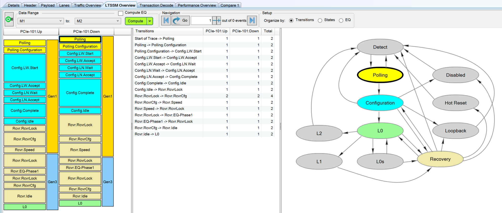
Each state also has conditions that trigger transitions to other states. All this is typically implemented in gate-level logic (HDL), not software, although there may be software hooks that can trigger state transitions manually. The top-level LTSSM diagram looks like this:
The entry point after a reset is the Detect state and the normal progression is through Detect, Polling, and Configuration, to the golden state of L0, the Link Up state where application data can be exchanged. This happens first at Gen1 speed (2.5GT/s). If both link partners support a higher speed, they can enter the Recovery state, change speeds, then return to L0 at the higher speed.
Each of these top-level states has a number of substates that define actions and conditions for transitioning between substates or moving to the next top-level state. The following sections detail the substates in the normal path from Detect to L0, including a speed change through Recovery. Not covered are side paths such as low-power states (L0s, L1, L2), since just the main path is complex enough for one post.
Detect
The Detect state is the only one that doesn't involve sending or receiving Ordered Sets. Its purpose is to periodically look for receiver termination, indicating the presence of a link partner. This is done with an implementation-specific analog mechanism built into the PHY.
Detect.Quiet
This is the entry point of the LTSSM after a reset and the reset point after many timeout or fault conditions. Software can also force the LTSSM back into this state to retrain the link. The transmitter is set to electrical idle. In
PG239, this is done by setting the
phy_txelecidle bit for each lane. The LTSSM stays in this state until 12ms have elapsed or the receiver detects that any lane has exited electrical idle (
phy_rxelecidle goes low). Then, it will proceed to
Detect.Active.
In the absence of a link partner, the LTSSM will cycle between Detect.Quiet and Detect.Active with a period of approximately 12ms. This period, as well as other timeouts in PCIe, are specified with a tolerance of (+50/-0)%, so it can really be anywhere from 12-18ms. This allows for efficient logic for counter comparisons. For example, with a PHY clock of 125MHz, a count of 2^17 is 1.049ms, so a single 6-input LUT attached to counter[22:17] can just wait for 6'd12 and that will be an accurate-enough 12ms timeout trigger.
Detect.Active
The transmitter for each lane attempts to detect receiver termination on that lane, indicating the presence of a link partner. This is done by measuring the time constant of the RC circuit created by the Tx AC-coupling capacitor and the Rx termination resistor. In
PG239, the MAC sets the signal
phy_txdetectrx and monitors the result in
phy_rxstatus on each lane.
There are three possible outcomes:
- No receiver termination is detected on any lane. The LTSSM returns to Detect.Quiet.
- Receiver termination is detected on all lanes. The LTSSM proceeds to Polling on all lanes.
- Receiver termination is detected on some, but not all, lanes. In this case, the link partner may have fewer lanes. The transmitter waits 12ms, then repeats the receiver detection. If the result is the same, the LTSSM proceeds to Polling on only the detected lanes. Otherwise, it returns to Detect.Quiet.
Polling
In Polling and most other states, link partners exchange Ordered Sets, easy-to-identify fixed-length packets containing link configuration information. They are transmitted in parallel on all lanes that detected receiver termination, although the contents may very per-lane in some states. The most important Ordered Sets for training are Training Sequence 1 (TS1) and Training Sequence 2 (TS2), 16-symbol packets with the following layouts:
 |
TS1 Ordered Set Structure
|
 |
| TS2 Ordered Set Structure |
In the Link Number and Lane Number fields, a special symbol (PAD) is reserved for indicating that the field has not yet been configured. This symbol has a unique 8b/10b control code (K23.7) in Gen1/2, but is just defined as 8'hF7 in Gen3. Polling always happens at Gen1 speeds (2.5GT/s).
Polling.Active
The transmitter sends TS1s with PAD for the Link Number and Lane Number. The receiver listens for TS1s or TS2s from the link partner.
The LTSSM normally proceeds to Polling.Configuration when all of the following conditions are met:
- Software is not commanding a transition to Polling.Compliance via the Enter Compliance bit in the Link Control 2 register.
- At least 1024 TS1s have been transmitted.
- Eight consecutive TS1s or TS2s have been received with Link Number and Lane Number set to PAD on all lanes, and not requesting Polling.Compliance unless also requesting Loopback (an unusual corner case).
If the above three conditions are not met on all lanes after 24ms timeout, the LTSSM proceeds to Polling.Configuration anyway if at least one lane received the necessary TS1s and enough lanes to form a valid link have exited electrical idle. Otherwise, it will assume it's connected to a passive test load and go to Polling.Compliance, a substate used to test compliance with the PCIe PHY specification by transmitting known sequences.
Polling.Configuration
The transmitter sends TS2s with PAD for the Link Number and Lane Number. The receiver listens for TS2s (not TS1s) from the link partner.
The LTSSM normally proceeds to Configuration when all of the following conditions are met:
- At least 16 TS2s have been transmitted after receiving one TS2.
- Eight consecutive TS2s have been received with Link Number and Lane Number set to PAD on any lane.
Unlike in Polling.Active, transmitted TS are only counted after receiving at least one TS from the link partner. This mechanism acts as a synchronization gate to ensure that both link partners receive more than enough TS to clear the state, regardless of which entered the state first.
If the above two conditions are not met after a 48ms timeout, the LTSSM returns to Detect and starts over.
Configuration
The downstream-facing (host/root complex) port leads configuration, proposing link and lane numbers based on the available lanes. The upstream-facing (device/end-point) port echoes back configuration parameters, if they are accepted. The following diagram and description are from the point of view of the downstream-facing port.
Configuration.Linkwidth.Start
The (downstream-facing) transmitter sends TS1s with a Link Number (arbitrary, 0-31) and PAD for the Lane Number. The receiver listens for matching TS1s.
The LTSSM normally proceeds to Configuration.Linkwidth.Accept when the following condition is met:
- Two consecutive TS1s are received with Link Number matching that of the transmitted TS1s, and PAD for the Lane Number, on any lane.
It the above condition is not met after a 24ms timeout, the LTSSM returns to Detect and starts over.
Configuration.Linkwidth.Accept
The downstream-facing port must decide if it can form a link using the lanes that are receiving a matching Link Number and PAD for the Lane Numbers. If it can, it assigns sequential Lane Numbers to those lanes. For example, an x4 link can be formed by assigning Lane Numbers 0-3.
The LTSSM normally proceeds to Configuration.Lanenum.Wait when the following condition is met:
- A link can be formed with a subset of the lanes that are responding with a matching Link Number and PAD for the Lane Numbers.
An interesting question is how to handle a case where only some of the detected lanes have responded. Should the LTSSM wait at least long enough to handle a missed packet and/or lane-to-lane skew before exiting this state? (I don't actually know the answer, but to me it seems logical to wait for at least a few TS periods before proposing lane numbers.)
If the above condition isn't met after a 2ms timeout, the LTSSM returns to Detect and starts over.
Configuration.Lanenum.Wait
The transmitter sends TS1s with the Link Number and with each lane's proposed Lane Number. The receiver listens for TS1s with a matching Link Number and updated Lane Numbers.
The LTSSM normally proceed to Configuration.Lanenum.Accept when the following condition is met:
- Two consecutive TS1s are received with Link Number matching that of the transmitted TS1s and with a Lane Number that has changed since entering the state, on any lane.
Here the spec is more explicit that upstream-facing lanes may take up to 1ms to start echoing the lane numbers, to account for receiver errors or lane-to-lane skew. So (I think) the above condition is meant to be evaluated only after 1ms has elapsed in this state.
If the above condition isn't met after a 2ms timeout, the LTSSM returns to Detect and starts over.
Configuration.Lanenum.Accept
Here, there are three possibilities:
- The updated Lane Numbers being received match those transmitted on all lanes, or the reverse (if supported). The LTSSM proceeds to Configuration.Complete.
- The updated Lane Numbers don't match the those transmitted, or the reverse (if supported). But, a subset of the responding lanes can be used to form a link. The downstream-facing port reassigns lane numbers for this new link and returns to Configuration.Lanenum.Wait.
- No link can be formed. The LTSSM returns to Detect and starts over.
Normally, lane reversal (e.g. 0-3 remapped to 3-0) would be handled by the device if it supports the feature, and its upstream-facing port will respond with matching Lane Numbers. However, if the device doesn't support lane reversal, it can respond with the reversed lane numbers to request the host do the reversal, if possible.
Configuration.Complete
The transmitter sends TS2s with the agreed-upon Link and Lane Numbers. The receiver listens for TS2s with the same.
The LTSSM normally proceeds to Configuration.Idle when all of the following conditions are met:
- At least 16 TS2s have been transmitted after receiving one TS2, on all lanes.
- Eight consecutive TS2s have been received with the same Link and Lane Numbers as are being transmitted, on all lanes.
If the above condition isn't met after a 2ms timeout, the LTSSM returns to Detect and starts over.
Configuration.Idle
The transmitter sends Idle data symbols (IDL) on all configured lanes. The receiver listens for the same. Unlike Training Sets, these symbols go through
scrambling, so this state also confirms that scrambling is working properly in both directions.
The LTSSM normally proceeds to L0 when all of the following conditions are met:
- At least 16 consecutive IDL have been transmitted after receiving one IDL, on all lanes.
- Eight consecutive IDL have been received, on all lanes.
If the above conditions aren't met after a 2ms timeout, the LTSSM returns to Detect and starts over.
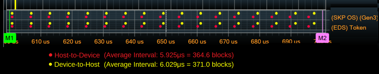
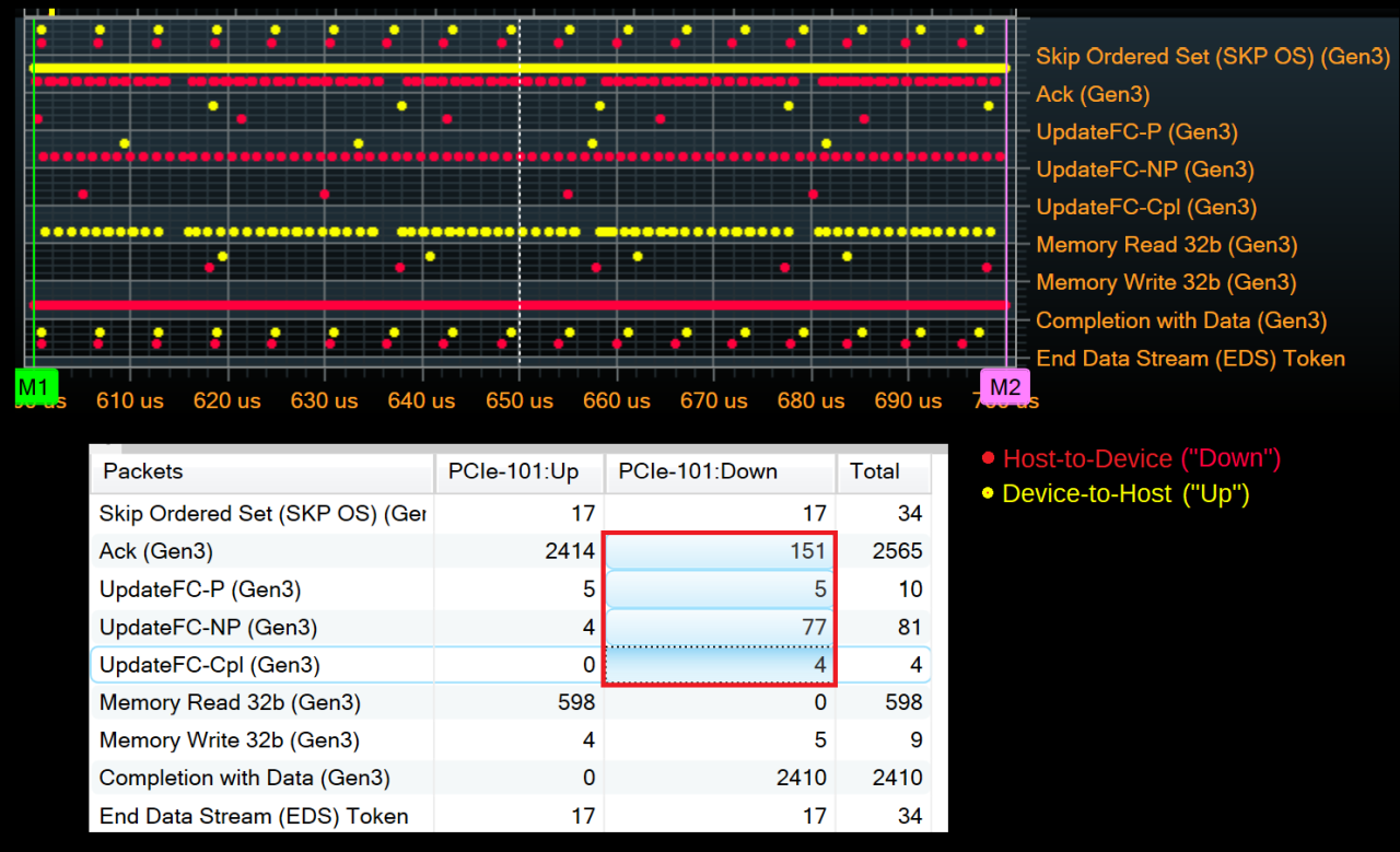
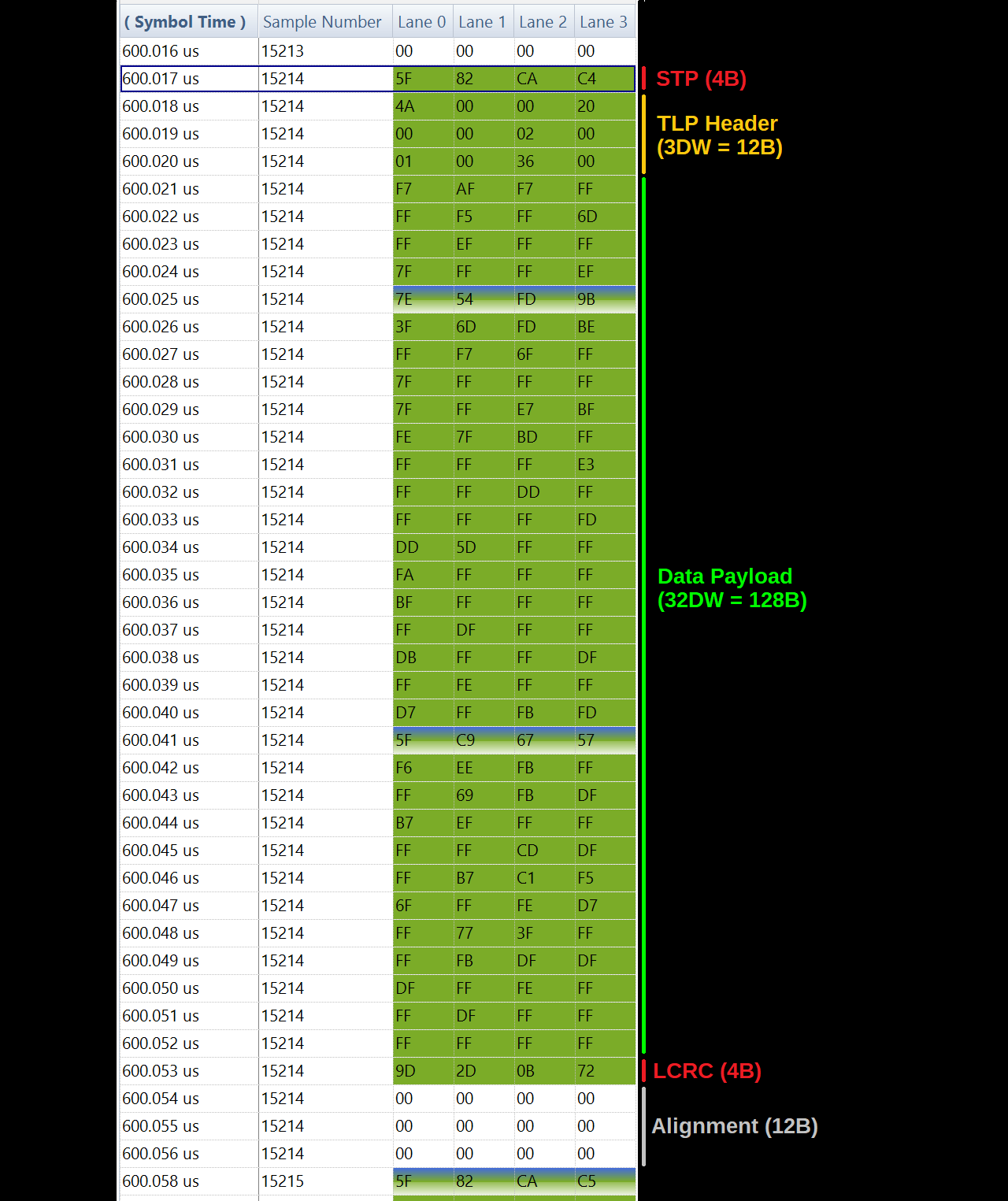
L0
This is the golden normal operational state where the host and device can exchange actual data packets. The LTSSM indicates Link Up status to the upper layers of the
stack, and they begin to do their work. One of the first things that happens after Link Up is flow control initialization by the Data Link Layer partners. Flow control is itself a state machine with some interesting rules, but that'll be for another post.
But wait...the link is still operating at 2.5GT/s at this point. If both link partners support higher data rates (as indicated in their Training Sets), they can try to switch to their highest mutually-supported data rate. This is done by transitioning to Recovery, running through the Recovery speed change substates, then returning to L0 at the new rate.
Recovery
Recovery is in many ways the most complex LTSSM state, with many internal state variables that alter state transitions rules and lead to circuitous paths through the substates, even for a nominal speed change. As with the other states, there are way too many edge cases to cover here, so I'll only focus on getting back to L0 at 8GT/s along the normal path.
Also, since Configuration has been completed, it's assumed that Link and Lane Numbers will match in transmitted and received Training Sequences. If this condition is violated, the LTSSM may fail back to Configuration or Detect depending on the nature of the failure. For simplicity, I'm omitting these paths from the descriptions of each substate.
When changing speeds to 8GT/s, the link must establish equalization settings during this state. In the simplest case, the downstream-facing port chooses a transmitter equalization preset for itself and requests a preset for the upstream-facing transmitter to use. The transmitter presets specify two parameters, de-emphasis and preshoot, that modify the shape of the transmitted waveform to counteract the low-pass nature of the physical channel. This can open the receiver eye even with lower overall voltage swing:
Recovery.RcvrLock
This substate is encountered (at least) three times.
The first time this substate is entered is from L0 at 2.5GT/s. The transmitter sends TS1s (at 2.5GT/s) with the Speed Change bit set. It can also set the EQ bit and send a Transmitter Preset and Receiver Preset Hint in this state. These presets are requested values for the upstream transmitter to use after it switches to 8GT/s. The receiver listens for TS1s or TS2s that also have the Speed Change bit set.
The first exit is normally to Recovery.RcvrCfg when the following condition is met:
- Eight consecutive TS1s or TS2s are received with the Speed Change bit matching the transmitted value (1, in this case), on all lanes.
The second time this subtstate is entered is from Recovery.Speed, after the speed has changed from 2.5GT/s to 8GT/s. Now, the link needs to be re-established at the higher data rate. Transitioning to 8GT/s always requires a trip through the equalization substate, so after setting its transmitter equalization, the LTSSM proceeds to Recovery.Equalization immediately.
The third time this subtstate is entered is from Recovery.Equalization, after equalization has been completed. The transmitter sends TS1s (at 8GT/s) with the Speed Change bit cleared, the EC bits set to 2'b00, and the equalization fields reflecting the downstream transmitter's current equalization settings: Transmitter Preset and Cursor Coefficients. The receiver listens for TS1s or TS2s that also have the Speed Change and EC bits cleared.
The third exit is normally to Recovery.RcvrCfg when the following condition is met:
- Eight consecutive TS1s or TS2s are received with the Speed Change bit matching the transmitted value (0, in this case), on all lanes.
Recovery.RcvrCfg
This substate is encoutered (at least) twice.
The first time this substate is entered is from Recovery.RcvrLock at 2.5GT/s. The transmitter sends TS2s (at 2.5GT/s) with the Speed Change bit set. It can also set the EQ bit and send a transmitter preset and receiver preset hint in this state. These presets are requested values for the upstream transmitter to use after it switches to 8GT/s. The receiver listens for TS2s that also have the Speed Change bit set.
The first exit is normally to Recovery.Speed when the following condition is met:
- Eight consecutive TS2s are received with the Speed Change bit set, on all lanes.
The second time this substate is entered is from Recovery.RcvrLock at 8GT/s. The transmitter sends TS2s (at 8GT/s) with the Speed Change bit cleared. The receiver listens for TS2s that also have the Speed Change bit cleared.
The second exit is normally to Recovery.Idle when the following condition is met:
- Eight consecutive TS2s are received with the Speed Change bit cleared, on all lanes.
Recovery.Speed
In this substate, the transmitter enters electrical idle and the receiver waits for all lanes to be in electrical idle. At this point, the transmitter changes to the new higher speed and configures its equalization parameters. In
PG239, this is done using the
phy_rate and
phy_txeq_X signals.
The LTSSM normally returns to Recovery.RcvrLock after waiting at least 800ns and not more than 1ms after all receiver lanes have entered electrical idle.
This state may be re-entered if the link cannot be reestablished at the new speed. In that case, the data rate can be changed back to the last known-good speed.
Recovery.Equalization
The Recovery.Equalization substate has phases, indicated by the Equalization Control (EC) bits of the TS1, that are themselves like sub-substates. From the point of view of the downstream-facing port, Phase 1 is always encountered, but Phase 2 and 3 may not be needed if the initially-chosen presets are acceptable.
In Phase 1, the transmitter sends TS1s with EC = 2'b01 and the equalization fields indicating the downstream transmitter's equalization settings and capabilities: Transmitter Preset, Full Scale (FS), Low Frequency (LF), and Post-Cursor Coefficient. The FS and LF values indicate the range of voltage adjustments possible for transmitter equalization.
The LTSSM normally returns to Recovery.RcvrLock when the following condition is met:
- Two consecutive TS1s are received with EC = 2'b01.
This essentially means that the presets chosen in the EQ TS1s and EQ TS2s sent at 2.5GT/s have been applied and are acceptable. If the above condition is not met after a 24ms timeout, the LTSSM returns to Recovery.Speed and changes back to the lower speed. From there, it could try again with different equalization presets, or accept that the link will run at a lower speed.
It's also possible for the downstream port to request further equalization tuning: In Phase 2 and Phase 3 of this substate, link partners can iteratively request different equalization settings and evaluate (via some implementation-specific method) the link quality. In a completely "known" link, these steps can be skipped if one of the transmitter presets has already been validated.
Recovery.Idle
This substate serves the same purpose as Configuration.Idle, but at the higher data rate (assuming the speed change was successful).
The transmitter sends Idle data symbols (IDL, 8'h00) on all configured lanes. The receiver listens for the same. These symbols now go through 8GT/s
scrambling, so this state also confirms that 8GT/s scrambling is working properly in both directions.
The LTSSM normally returns to L0 when all of the following conditions are met:
- At least 16 consecutive IDL have been transmitted after receiving one IDL, on all lanes.
- Eight consecutive IDL have been received, on all lanes.
If the above conditions aren't met after a 2ms timeout, the LTSSM returns to Detect and starts over.
LTSSM Protocol Analyzer Captures
There are lots of places for the LTSSM to go wrong, and since it's running near the very bottom of the stack, it's hard to troubleshoot without dedicated tools like a PCIe Protocol Analyzer. In my
tool hunt, I managed to get a used U4301B, so let's put it to use and look at some LTSSM captures.
Side note: Somebody just scored an insane deal on a dual U4301A
listing that included the unicorn U4322A probe. If you're that someone and you want to sell me just the probe, let me know! I will take it in any condition just for the spare pins. Also, there is a reasonably-priced
U4301B up right now if anyone's looking for one.
But anyway, my Frankenstein U4301B + M.2 interposer is still operational and can be used with the Keysight software to capture Training Sets and summarize LTSSM progress:
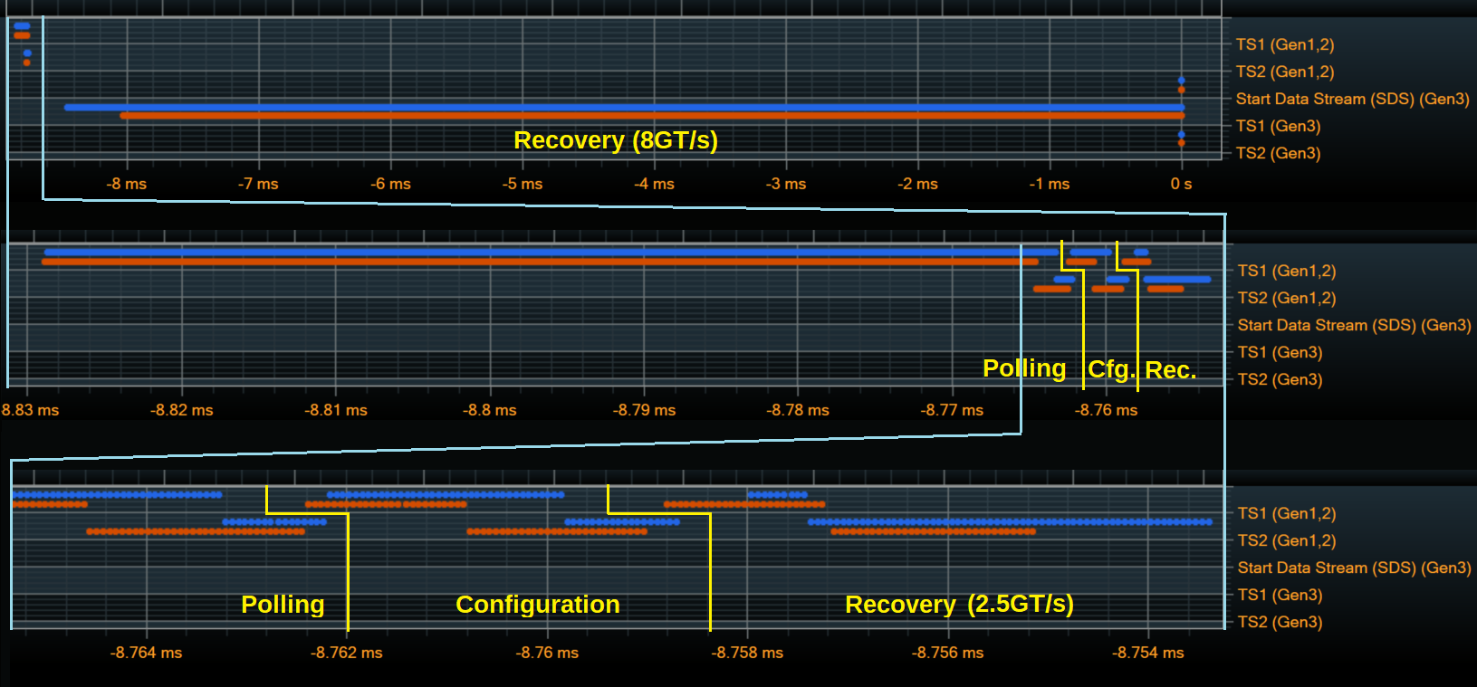
You can see the progression through Polling and Configuration, L0, Recovery, and back to L0. In Recovery, you can see the speed change and equalization loops, crossing through the base state of Recovery.RcvrLock three times as described above.
Looking at the Training Sequence traffic itself, the entire LTSSM takes around 9ms to complete in this example, with the vast majority of the time spent in the Recovery state after the speed change. Zooming in shows the details of the earlier states, down to the level of individual Training Sequences.
If any of the states transitions don't go as expected it's possible to look inside the individual Training Sequences to troubleshoot what conditions aren't being met. The exact timing and behavior varies a lot from device to device, though.
So you made it to L0...what next?
L0 / Link Up means the physical link is established, so the upper layers of the PCIe stack can begin to communicate across the link. However, before any application data (memory transactions) can be transferred, the Data Link Layer must initialize flow control. PCIe flow control is itself an interesting topic that deserves a separate post, so I'll end here for now!