Before getting too caught up in the inner workings of PCIe, it's probably worth taking a look at the high-level architecture - how it's used in a system and what the PCIe controller stack looks like. PCIe is fundamentally a bi-directional memory bus extension: it allows the host to access memory on a device and a device to access memory on the host.
When a PCIe link is established between the host and a device, the host assigns address space(s) that it can use to access device memory. Optionally, it can also grant permission for the device to access portions of host system memory. In that way, the host and device memory buses are effectively connected. Each PCIe link is a point-to-point connection, but they can be combined with switches into a fabric with many devices (endpoints).
Different types of devices utilize the memory bus bridging capability of PCIe in different ways. For example, an NVMe storage device exposes only a small amount of device memory (the NVMe Controller Registers) that the host uses to configure the device and inform it when new commands have been submitted. All actual data transfer is done by the storage device reading from or writing to host memory. In this way, the NVMe storage device acts as a DMA controller between host memory and non-volatile storage.
 |
| NVMe storage device usage of PCIe link (completion steps omitted). |
One might ask why the memory buses can't just be directly connected. For one, a native memory interface such as AXI is very wide: it might have 64-256b of data, 32-64b of address, and a bunch of control signals. This works fine inside a chip, but going from chip-to-chip, board-to-board, or across a cable, it's too many signals. The PCIe Controller encapsulates the data, address, and control signals from the memory bus into packets that can be sent across a fast serial link over a small number of differential pairs. This standard interface also allows bridging memory buses with different native interfaces, speeds, and latencies.
With that context in mind, we can look at the PCIe Controller stack, and what role each layer plays in bridging memory transactions between the host and device as efficiently and reliably as possible. The PCIe specification defines three layers: the Transaction Layer (TXL), the Data Link Layer (DLL), and the Physical Layer (PHY). These layers each have a transmit and a receive side. From the point of view of the host, the stack looks like this:
Memory transactions from the host to the device are packaged by the TXL into a Transaction Layer Packet (TLP) with a header containing the address and other control information. The DLL prepends a framing token (STP) and appends a CRC to the TLP to create a Link Packet. This is then split into lanes and serialized by the PHY. The process happens in reverse for memory transactions from device to host, to go from serialized Link Packets back to host memory transactions.
In practice, many architectures (including Ultrascale+) break the PHY into two parts: an upper Media Access Control (MAC) layer and a lower layer still called the PHY. These are connected by the standard PHY Interface for PCI Express (PIPE), published by Intel. It's also useful to add an explicit AXI-PCIe bridge layer above the TXL when the native memory bus is AXI, as it is in the Ultrascale+ architecture. This would be an example of what some references call the Application Layer. Expanded this way, the stack looks like this:
Different Xilinx IPs cover different layers of the stack, as shown above. PG239 (PCI Express PHY) is a low-level (PIPE down) PCIe PHY wrapper for the GTH/GTY serial transceivers. PG213 (UltraScale+ Devices Integrated Block for PCI Express) covers the PCIE4 hardware block that includes the TXL, DLL, and MAC layers, and interfaces to the PHY via PIPE. And PG194 (AXI Bridge for PCI Express Gen3 Subsystem) includes the AXI-PCIe bridge layer on top of the PCIE4 hardware block and PHY. (For Ultrascale+, this is technically implemented as a configuration of PG195, but the relevant documentation is still in PG194.)
All of these Xilinx IPs are included in Vivado at no additional cost, but not every device has the PCIE4 block(s) needed to instantiate PG213 or PG194/PG195. For the Zynq Ultrascale+ line, the product tables show how many PCIe lanes are supported by integrated PCIE4 blocks for each device. In general, the larger and more expensive chips have more available PCIe hardware. But there are exceptions like the ZU6xx, ZU9xx, and ZU15xx, which have none. These can still instantiate PG239, but require a PCIe soft IP to implement the rest of the stack.
Each layer communicates with the next through a data bus that's sized to match the speed of the link. The example above is for a Gen3 x4 link, which supports 32Gb/s of serial data in each direction. In the Ultrascale+ implementation, the 250MHz clock for the 128b internal datapath is derived from the PCIe reference clock, so all layer logic is synchronous with the PHY. This seems like a perfectly-balanced data pipeline, with 32Gb/s of data coming in and going out in each direction. But in practice, overheads limit the maximum link efficiency.
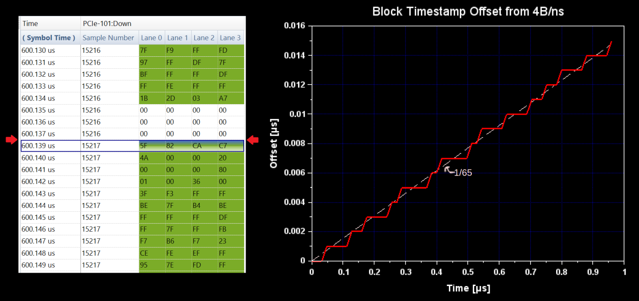
First, PCIe Gen3 uses 128b/130b encoding: for each 128b serial data payload on each lane, a 2b sync header is prepended to create a 130b block. The sync bits tell the receiver whether the block is data or an Ordered Set (control sequence). In order to make room for the sync bits, PIPE requires one invalid data clock cycle in every 65-clock period.
The period for skipping data on the 250MHz side of the PHY is 260ns, while the period for a 130b serial output block is only 16.25ns, so the PHY must implement buffering and a SERDES gearbox to make this work. The effect of the sync bits can be seen in the protocol analyzer raw data, where there are occasionally 1ns gaps in the timestamp. (The full serial data rate including sync bits would be exactly 4B/ns.) These leap-nanoseconds add up to an overall efficiency of 98.5% (64/65), as can be seen by plotting the starting timestamp of each block.

Next, transmitters are required to periodically stop transmitting data and send a SKP Ordered Set (SKP OS), which is used to compensate for clock drift. This should happen every 370-375 blocks, and the SKP OS takes one block to transmit. Stopping the data stream also requires sending an EDS token, which may require one additional block depending on packet alignment. But even in a worst-case scenario this still represents about 99.5% (368/370) efficiency.
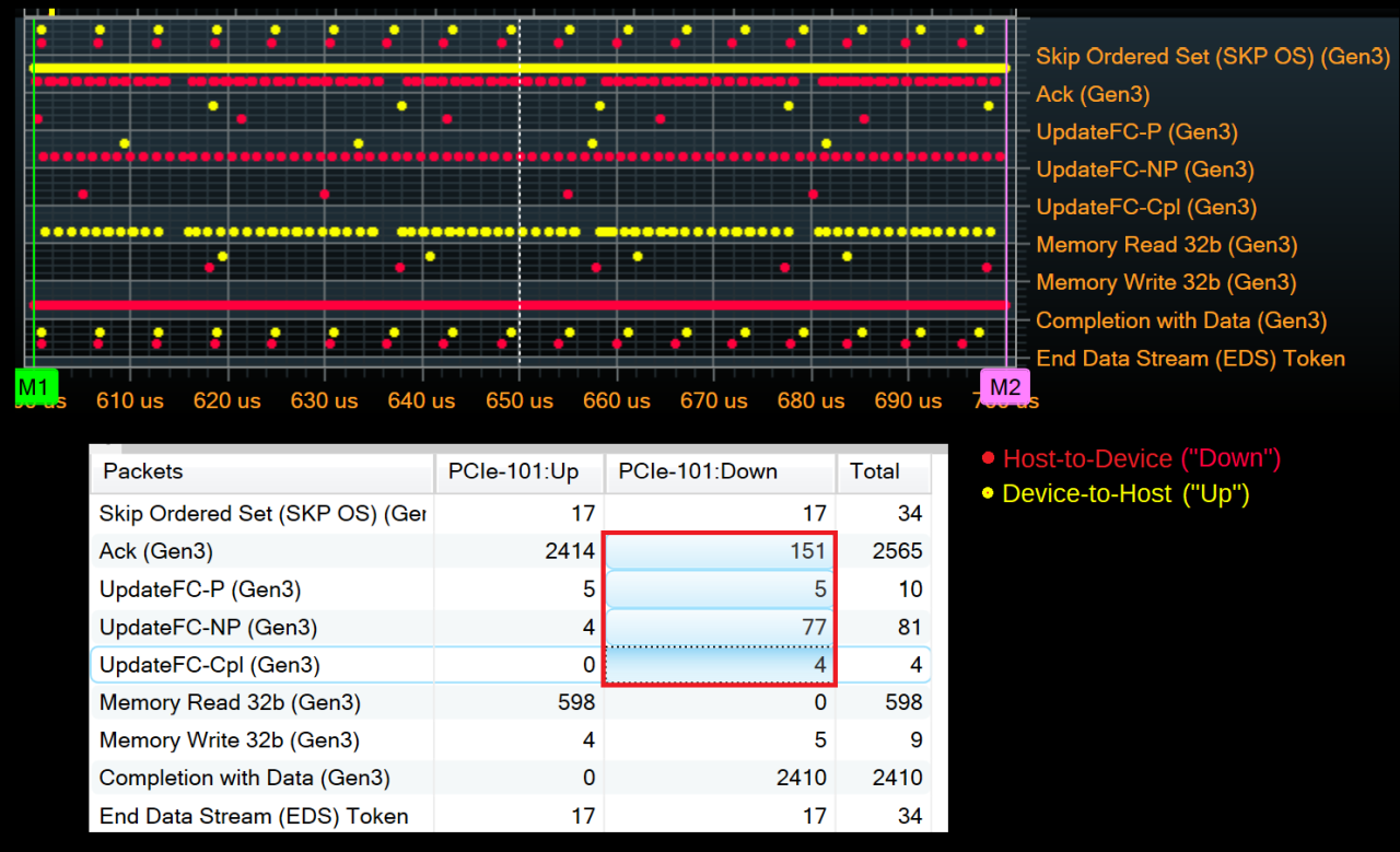
We can see the EDS tokens and SKP OS at regular intervals in both directions on the protocol analyzer. Interestingly, the average interval in the Host-to-Device direction is on the short side (365 blocks). Maybe it's not accounting for the 64/65 PIPE TxDataValid efficiency described above. The interval is controlled by the MAC layer, which is in PG213 in this case, so I don't think it's something that can be adjusted. The Device-to-Host direction is spot-on in this case, with a 371-block interval.

DLLs also exchange Data Link Layer Packets (DLLPs) for Ack/Nak and flow control of TLPs. These packets are short (6B), but they must be transmitted with enough regularity to meet latency requirements and ensure receiver buffers don't overflow. There's no simple rule for when these are transmitted, only a set of constraints based on the link operating conditions. To get a feel for the typical link efficiency impact of DLLP traffic, we can look at a 100μs section of bulk data transfer and add up the combined contribution of all DLLPs:

In total, there were 237 DLLPs transmitted in the Host-to-Device direction. Since the packets must be lane-0-aligned on an x4 link, they actually occupy 8B each. This is 1896B of overhead for nearly 400000B of data, again around 99.5% efficiency. This example is mostly unidirectional data transfer from host to device, though. If the device was also sending data to the host, there would be far more Acks going in the Host-to-Device direction. If the Ack count were similar to that of the Device-to-Host direction in this example, the efficiency would drop to around 95%.
Lastly, the biggest overhead is usually for TLP packetization. The TLP header is either 12B or 16B. The DLL adds a 4B framing token (STP) and a 4B Link CRC (LCRC). The payload size can be as high as 4096B, although it's limited to 1024B in the Ultrascale+ implementation (PG213). It's also common for devices to limit the max payload size to 128B, 256B, or 512B, depending on the capability of their PCIe Controller. This gives a range of 84.2% (128/150) to 98.1% (1024/1044) for packetization efficiency with optimally-sized transfers on Ultrascale+ hardware.
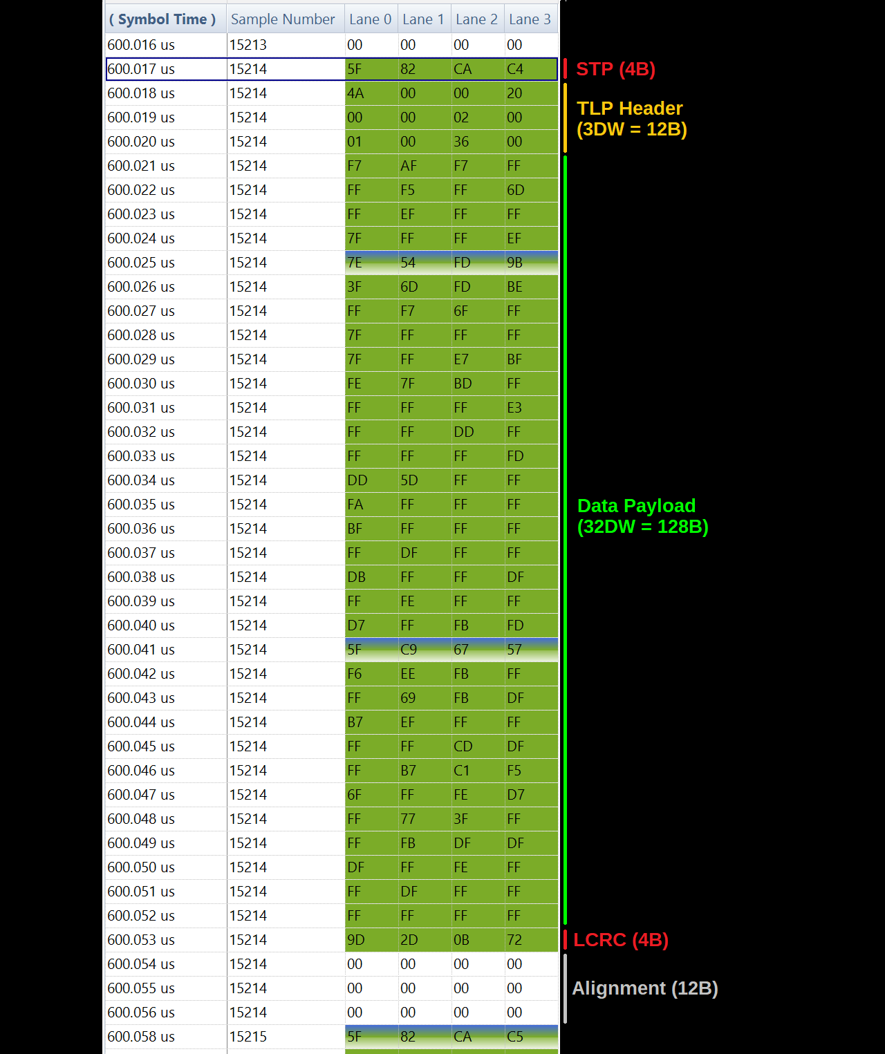
In the example capture, data is transferred from host to device in 128B-payload TLPs:

The packet has 20B of overhead for 128B of data, which would be an 86.5% efficiency. However, the host controller also inserts 12B of logical idle (zeros) to align the next STP token to the start of a block. This isn't required by the PCIe protocol, but may be inherent in the implementation of the controller. For this payload size, it drops the efficiency to 80% (128/160).
That packetization efficiency dominates the overall link efficiency, which hovers between 75% and 80% during periods of stable data transfer:

In this case, increasing the max payload size would have the most positive impact on throughput. PG213 can go up to 1024B, but the device controller may be the limiting factor.
In PCIe 6.0, a big change will be introduced that removes sync bits and consolidates DLLPs, framing tokens, and the LCRC into a fixed 20B overhead in each 256B unit (called a FLIT, for Flow Control unIT). This implies a fixed 92.2% efficiency for everything other than the SKP OS and TLP header overhead, and also a fixed latency for Ack/Nak and flow control, a nice simplification.
But for now we're still in the realm of PCIe Gen3, where we can expect an overall link efficiency in the 75-95% range, depending on the variety of factors described above as well as details of the controller implementations.
The packetization and flow control functions described above are the domain of the Transaction Layer and Data Link Layer, but there are also some really interesting functions of the MAC and PHY layers that facilitate reliable serial data transfer across the physical link. These will have to be topics for one or more future posts, though.


