Tuesday, August 22, 2023

PCIe Deep Dive, Part 3: Scramblers, CRCs, and the Parallel LFSR

This post continues an exploration into the inner workings of PCIe. The previous post presented a top-level view of the PCIe Controller as a memory bus extension, with discussion of the various overheads associated with wrapping memory transfers into serial data packets. In this post, I want go to the other extreme and look at one of the low-level logic mechanisms that PCIe depends on for reliable data transfer: the parallel Linear-Feedback Shift Register (LFSR). This mechanism efficiently introduces randomness required to ensure DC-balanced serial data, and to validate Transaction Layer Packets (TLPs) with a Cyclic Redundancy Check (CRC).

PCIe 3.0 Scrambler

PCIe signals are driven across AC-coupled differential pairs to increase immunity to noise. The transmitter and receiver may be on different boards, far apart from each other, with significant high-frequency ground offset between them. Adding series capacitors to the differential signal provides low-voltage level shifting capability to deal with this. But, this only works if the data coming across the link is DC-balanced over a data interval much shorter than the time constant formed by the AC coupling capacitor and termination resistor, which is typically 10⁴ to 10⁵ UI.

PCIe 1.0 and 2.0 use 8b/10b encoding to enforce DC balance. This encoding tracks the running disparity of the serial data stream and modifies 10b symbols (representing 8b data) to keep it in balance. This is also the encoding used in USB all the way up to USB 3.x Gen 1 (5Gbps), which is the same speed as PCIe 2.0. It's simple and deterministic, but it has a poor serial encoding efficiency of only 80% (8/10).

By contrast, PCIe 3.0 through PCIe 5.0 use 128b/130b encoding, where two sync bits are prepended to 128b data payloads to form 130b blocks. As discussed in the previous post, this has a much better serial encoding efficiency of 98.5% (128/130). However, the two sync bits are not sufficient to control running disparity with a 128b data payload. Instead, the data is sent through a scrambler, a Pseudo-Random Number Generator (PRNG) that remaps bits in a way that both the transmitter and receiver understand. The output stream is statistically DC-balanced for all real data.

The PCIe implementation of the PRNG for scrambling is as a Linear-Feedback Shift Register (LFSR). In the case of PCIe 3.0, the canonical implementation is a 23-bit shift register with strategically-placed XORs between some bits to instigate pseudo-randomness. The output of the shift register is then XORed with each data bit to generate the scrambled output. Each lane gets its own LFSR scrambler seeded with a different value.

This is simple logic, but it would need to run at 8GHz to be implemented in single-bit fashion like this. That's not really practical even in dedicated silicon, and is completely impossible using FPGA sequential logic. However, it's possible to parallelize the LFSR to any data width pretty easily. The key is in the name: the operation is linear, so the contributions of each bit of input data and the initial LFSR can be superimposed to generate each bit of output data and the final LFSR. This method of parallelizing the LFSR is covered very well at OutputLogic.com, with utilities to generate Verilog implementations of any LFSR and data width. I will only briefly describe the procedure here.

Using for example the 23-bit LFSR and a 32-bit data path (common for each PCIe 3.0 lane with a 250MHz PHY clock), there are a total of 23 + 32 = 55 bits that can contribute to the final LFSR and output data. Set each of those bits to one, and all other bits to zero, then run the LFSR forward by 32 steps, and record the contribution of each input bit to the output data and final LFSR. This creates a big table of bit contributions:

The full parallel operation is just the sum (in mod 2, so XOR) of contributions from each bit of input data and the initial LFSR. Each bit of the output data and final LFSR is the XOR combination of a specific set of input bits, with at most 55 contributing bits. On a Xilinx Ultrascale+ FPGA, wide XORs like this are easy to build using nested six-input LUTs. With two levels, you get 6² = 36 inputs. With three levels, 6³ = 216 inputs. Each level has a propagation time on the order of 1ns, so even nested three deep it's capable of running at 250MHz.

Link CRC

Another use for the parallel LFSR is in the generation and checking of the Link CRC, a 32-bit value used for error detection in TLPs. The LCRC acts like a signature for the bits in the TLP and the value received must match the value calculated by the receiver, or the TLP is rejected. The LCRC mechanism uses a 32-bit LFSR (with XOR positions described by the standard CRC-32 polynomial 0x04C11DB7), seeded to 0xFFFFFFFF at the start of each TLP. At the end of the TLP, the 32-bit LFSR value is mapped to the packet's LCRC through some additional bit manipulation.

The LCRC operation can be parallelized in the same way as the Scrambler. The main differences are that the data is unmodified by the LCRC operation and that the data does contribute to the XOR sum of the next LFSR value. (This is what drives the LCRC to a unique value for each TLP.) In table form, this just changes which quadrants have XOR contributions:

Although there are fewer rows to handle, there are now 128 + 32 = 160 columns. The LCRC is calculated on packets before they are striped across all lanes. So for a PCIe 3.0 x4 link, instead of four 32-bit data paths as in the Scrambler, there is just one 128b data path operating at 250MHz. Any of these bits and any of the 32 bits of the previous clock cycle's LFSR might contribute to the XOR for each bit of the new LFSR. This isn't a problem, though, since three levels of LUT6 can handle up to 216 XOR inputs at 250MHz, as described above.

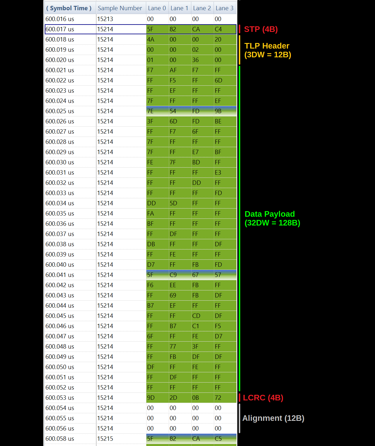
Where things do get a little complicated is in data alignment. TLP lengths are multiples of one Double Word (DW), or 32b. So, even without considering framing, 3/4 of the possible lengths would not fit evenly into 128b data beats. Each TLP is also prepended with a 32-bit framing token (STP), the latter half of which is fed into the LCRC computation as well. So in fact all cases will involve a partial data beat.

To handle this with a 128b parallel LFSR, the LCRC mechanism must get clever. Based on the length of the packet (which is known once the STP is parsed), the 128b data window can be shifted such that the last data beat will be aligned with the end of the packet. This ensures that the final LFSR value can be used directly to generate the LCRC. Then, the first 128b data beat is padded with zeros up to the middle of the STP token, where the LCRC computation begins. (In the case of a 3DW header with no data, the first and last data beat are the same.) This creates four possible alignment cases that repeat based on the length of the TLP:

Depending on the alignment case, the LFSR is seeded with a different value that accounts for the extra {16, 48, 80, 112} zeros padded onto the first data beat. These seed values are derived by seeding the reference single-bit implementation of the LFSR with 0xFFFFFFFF, then running it backwards for {16, 48, 80, 112} steps with zero data bits. With these seeds, the 128b parallel LFSR can be run on the zero-padded data and give the same final result as the single-bit implementation on the original data.

An interesting follow-up issue is how to handle back-to-back TLPs. Padding the first LCRC beat with zeros potentially means more than a 1:1 bit rate for the LCRC engine compared to the packet data, if there is no idle time between packets. An easy workaround could be to run two LCRC engines that take turns processing packets, although this means twice the logic area. The details are likely to vary in every implementation, so it's not something I will get into here.

Conclusion

The last couple of posts were setup and background for PCIe in general. This one was more of a microscopic view of a particular logic mechanism key to several aspects of PCIe, and how it can be implemented efficiently on modern FPGAs. There are many such interesting logic puzzles to solve in gateware implementations of PCIe, and I wanted to give just one example at the lowest level I understand. I may cover other logic-level tricks in future posts, but first I think it will be more interesting to introduce what might be the scariest part of PCIe: the Link Training and Status State Machine (LTSSM). To be continued...

Sunday, June 11, 2023

PCIe Deep Dive, Part 2: Stack and Efficiency

Before getting too caught up in the inner workings of PCIe, it's probably worth taking a look at the high-level architecture - how it's used in a system and what the PCIe controller stack looks like. PCIe is fundamentally a bi-directional memory bus extension: it allows the host to access memory on a device and a device to access memory on the host.

When a PCIe link is established between the host and a device, the host assigns address space(s) that it can use to access device memory. Optionally, it can also grant permission for the device to access portions of host system memory. In that way, the host and device memory buses are effectively connected. Each PCIe link is a point-to-point connection, but they can be combined with switches into a fabric with many devices (endpoints).

Different types of devices utilize the memory bus bridging capability of PCIe in different ways. For example, an NVMe storage device exposes only a small amount of device memory (the NVMe Controller Registers) that the host uses to configure the device and inform it when new commands have been submitted. All actual data transfer is done by the storage device reading from or writing to host memory. In this way, the NVMe storage device acts as a DMA controller between host memory and non-volatile storage.

NVMe storage device usage of PCIe link (completion steps omitted).

One might ask why the memory buses can't just be directly connected. For one, a native memory interface such as AXI is very wide: it might have 64-256b of data, 32-64b of address, and a bunch of control signals. This works fine inside a chip, but going from chip-to-chip, board-to-board, or across a cable, it's too many signals. The PCIe Controller encapsulates the data, address, and control signals from the memory bus into packets that can be sent across a fast serial link over a small number of differential pairs. This standard interface also allows bridging memory buses with different native interfaces, speeds, and latencies.

With that context in mind, we can look at the PCIe Controller stack, and what role each layer plays in bridging memory transactions between the host and device as efficiently and reliably as possible. The PCIe specification defines three layers: the Transaction Layer (TXL), the Data Link Layer (DLL), and the Physical Layer (PHY). These layers each have a transmit and a receive side. From the point of view of the host, the stack looks like this:

Memory transactions from the host to the device are packaged by the TXL into a Transaction Layer Packet (TLP) with a header containing the address and other control information. The DLL prepends a framing token (STP) and appends a CRC to the TLP to create a Link Packet. This is then split into lanes and serialized by the PHY. The process happens in reverse for memory transactions from device to host, to go from serialized Link Packets back to host memory transactions.

In practice, many architectures (including Ultrascale+) break the PHY into two parts: an upper Media Access Control (MAC) layer and a lower layer still called the PHY. These are connected by the standard PHY Interface for PCI Express (PIPE), published by Intel. It's also useful to add an explicit AXI-PCIe bridge layer above the TXL when the native memory bus is AXI, as it is in the Ultrascale+ architecture. This would be an example of what some references call the Application Layer. Expanded this way, the stack looks like this:

Different Xilinx IPs cover different layers of the stack, as shown above. PG239 (PCI Express PHY) is a low-level (PIPE down) PCIe PHY wrapper for the GTH/GTY serial transceivers. PG213 (UltraScale+ Devices Integrated Block for PCI Express) covers the PCIE4 hardware block that includes the TXL, DLL, and MAC layers, and interfaces to the PHY via PIPE. And PG194 (AXI Bridge for PCI Express Gen3 Subsystem) includes the AXI-PCIe bridge layer on top of the PCIE4 hardware block and PHY. (For Ultrascale+, this is technically implemented as a configuration of PG195, but the relevant documentation is still in PG194.)

All of these Xilinx IPs are included in Vivado at no additional cost, but not every device has the PCIE4 block(s) needed to instantiate PG213 or PG194/PG195. For the Zynq Ultrascale+ line, the product tables show how many PCIe lanes are supported by integrated PCIE4 blocks for each device. In general, the larger and more expensive chips have more available PCIe hardware. But there are exceptions like the ZU6xx, ZU9xx, and ZU15xx, which have none. These can still instantiate PG239, but require a PCIe soft IP to implement the rest of the stack.

Each layer communicates with the next through a data bus that's sized to match the speed of the link. The example above is for a Gen3 x4 link, which supports 32Gb/s of serial data in each direction. In the Ultrascale+ implementation, the 250MHz clock for the 128b internal datapath is derived from the PCIe reference clock, so all layer logic is synchronous with the PHY. This seems like a perfectly-balanced data pipeline, with 32Gb/s of data coming in and going out in each direction. But in practice, overheads limit the maximum link efficiency.

First, PCIe Gen3 uses 128b/130b encoding: for each 128b serial data payload on each lane, a 2b sync header is prepended to create a 130b block. The sync bits tell the receiver whether the block is data or an Ordered Set (control sequence). In order to make room for the sync bits, PIPE requires one invalid data clock cycle in every 65-clock period.

The period for skipping data on the 250MHz side of the PHY is 260ns, while the period for a 130b serial output block is only 16.25ns, so the PHY must implement buffering and a SERDES gearbox to make this work. The effect of the sync bits can be seen in the protocol analyzer raw data, where there are occasionally 1ns gaps in the timestamp. (The full serial data rate including sync bits would be exactly 4B/ns.) These leap-nanoseconds add up to an overall efficiency of 98.5% (64/65), as can be seen by plotting the starting timestamp of each block.

Next, transmitters are required to periodically stop transmitting data and send a SKP Ordered Set (SKP OS), which is used to compensate for clock drift. This should happen every 370-375 blocks, and the SKP OS takes one block to transmit. Stopping the data stream also requires sending an EDS token, which may require one additional block depending on packet alignment. But even in a worst-case scenario this still represents about 99.5% (368/370) efficiency.

We can see the EDS tokens and SKP OS at regular intervals in both directions on the protocol analyzer. Interestingly, the average interval in the Host-to-Device direction is on the short side (365 blocks). Maybe it's not accounting for the 64/65 PIPE TxDataValid efficiency described above. The interval is controlled by the MAC layer, which is in PG213 in this case, so I don't think it's something that can be adjusted. The Device-to-Host direction is spot-on in this case, with a 371-block interval.

DLLs also exchange Data Link Layer Packets (DLLPs) for Ack/Nak and flow control of TLPs. These packets are short (6B), but they must be transmitted with enough regularity to meet latency requirements and ensure receiver buffers don't overflow. There's no simple rule for when these are transmitted, only a set of constraints based on the link operating conditions. To get a feel for the typical link efficiency impact of DLLP traffic, we can look at a 100μs section of bulk data transfer and add up the combined contribution of all DLLPs:

In total, there were 237 DLLPs transmitted in the Host-to-Device direction. Since the packets must be lane-0-aligned on an x4 link, they actually occupy 8B each. This is 1896B of overhead for nearly 400000B of data, again around 99.5% efficiency. This example is mostly unidirectional data transfer from host to device, though. If the device was also sending data to the host, there would be far more Acks going in the Host-to-Device direction. If the Ack count were similar to that of the Device-to-Host direction in this example, the efficiency would drop to around 95%.

Lastly, the biggest overhead is usually for TLP packetization. The TLP header is either 12B or 16B. The DLL adds a 4B framing token (STP) and a 4B Link CRC (LCRC). The payload size can be as high as 4096B, although it's limited to 1024B in the Ultrascale+ implementation (PG213). It's also common for devices to limit the max payload size to 128B, 256B, or 512B, depending on the capability of their PCIe Controller. This gives a range of 84.2% (128/150) to 98.1% (1024/1044) for packetization efficiency with optimally-sized transfers on Ultrascale+ hardware.

In the example capture, data is transferred from host to device in 128B-payload TLPs:

The packet has 20B of overhead for 128B of data, which would be an 86.5% efficiency. However, the host controller also inserts 12B of logical idle (zeros) to align the next STP token to the start of a block. This isn't required by the PCIe protocol, but may be inherent in the implementation of the controller. For this payload size, it drops the efficiency to 80% (128/160). 

That packetization efficiency dominates the overall link efficiency, which hovers between 75% and 80% during periods of stable data transfer:

In this case, increasing the max payload size would have the most positive impact on throughput. PG213 can go up to 1024B, but the device controller may be the limiting factor.

In PCIe 6.0, a big change will be introduced that removes sync bits and consolidates DLLPs, framing tokens, and the LCRC into a fixed 20B overhead in each 256B unit (called a FLIT, for Flow Control unIT). This implies a fixed 92.2% efficiency for everything other than the SKP OS and TLP header overhead, and also a fixed latency for Ack/Nak and flow control, a nice simplification.

But for now we're still in the realm of PCIe Gen3, where we can expect an overall link efficiency in the 75-95% range, depending on the variety of factors described above as well as details of the controller implementations.

The packetization and flow control functions described above are the domain of the Transaction Layer and Data Link Layer, but there are also some really interesting functions of the MAC and PHY layers that facilitate reliable serial data transfer across the physical link. These will have to be topics for one or more future posts, though.

Sunday, May 7, 2023

PCIe Deep Dive, Part 1: Tool Hunt

Over the past few years, I've been developing and improving very fast standalone NVMe-based storage capability for the Zynq Ultrascale+ architecture, to keep up with the absurd speeds of modern SSDs. (Drives like the Seagate Firecuda 530 and Sabrent Rocket 4 Plus-G can now hit 3GB/s+ sustained TLC write speeds, with much higher pSLC cache peaks.) But my knowledge pretty much ended at the interface to the Xilinx DMA/Bridge Subsystem for PCI Express (PG194/PG195). In the usual fashion, I'm now going to dive deeper to explore in more detail how the AXI-PCIe bridge works, and what the PCIe stack actually looks like.

Something I found interesting about PCIe in general is that there seems to be a pretty large barrier built up around the black box. Even just finding learning resources is much harder than it should be. The best I found was PCI Express Technology 3.0 and some accompanying material by MindShare, but even that seems like a prose wrapper on top of the specification. There isn't anything that I would consider a beginner's guide, like you might find for USB or Ethernet.

[Edit by Future Shane] There is a very good series of four articles from Simon Southwell starting here that offers a thorough introduction to PCIe. Definitely check it out if you're going to be exploring PCIe.

For physical tools, the situation is even more bleak. The speeds in PCIe Gen3 (8GT/s) put it in the range where an oscilloscope that can actually measure the signal will cost more than a car. But for all but the lowest-level hardware debugging, a digital capture would suffice, and that's where a protocol analyzer would be nice. Unfortunately, there is no Wireshark equivalent for PCIe; protocol analyzers for it are dedicated hardware that only a few companies develop, and they are priced astronomically.

That is...unless you scout them on eBay for a year.

Biggest "that escalated quickly" of my test equipment stack (ref. PicoScopes below table).

This is a used U4301B that I got in what has to be my second-best eBay score of all time, for less than it would have cost me to rent one for a month. There are only ever a handful of them up for auction at any given time, and the market is so small that the price is basically random, so if you're actually looking for one I can only wish you luck. This one goes up to Gen3 x8, which is fine for my purposes. If you only need Gen1/2 capability, the situation is much better.

[Edit by Future Shane] There is one listed on eBay for a good price right now if anyone else is looking for one. (I'll remove this note after it's no longer available.)

The U4301B is actually just the instrument in the bottom slot of the M9505A AXIe Chassis. This is meant to connect to a PCIe slot on a host machine using an iPass cable and interface card. Newer versions of the chassis controller have a laptop-friendly Thunderbolt connection instead. I "upgraded" mine using an eGPU enclosure, the smaller black box sitting on top.

I said that the U4301B was my second-best eBay score of all time, and that's because the number one is the U4322A probe that I got to go with it, from a different auction. The protocol analyzer is useless without a probe or interposer, and those are even harder to find used. I have never seen a U4322A on eBay before or since the one I got, and all other online listings for them are dead-ends. So the fact that I got one for what might as well be free compared to the new cost is just plain luck.

It was, however, a lot broken...

The probe has two rows of spring-loaded contacts that are meant to touch down on test pads for the PCIe signals. Unfortunately, mine was missing several pins and many others were bent or broken. It had been treated like a scrap cable, rather than a delicate probe. No problem, though, I can just replace the spring pins with some equivalent Mill-Max parts...

...oh, well shit.

This was one of the most ridiculous things I have ever seen under the microscope. Each spring pin has a surface-mount resistor soldered into its tip, and encased in epoxy. What the multi-GHz fuck is going on with these? Well, I suspect they each make up part of a passive probe, also called a Low-Z or Z0 probe. This video explains the concept in detail; it's forming a resistive divider with the 50Ω termination. But it must have extremely low capacitance on the input side of the resistor, hence the resistors embedded in the tips. The good news is that there are no amplifiers in the probe head, so there's not much else that can be broken.

There's no replacement for these pins, so the ones that were missing or broken were a lost cause. But luckily there were enough intact ones to make a full bidirectional x4 link, which is all I really needed. They weren't all in the right locations, so I had to carefully rearrange them with a soldering iron, taking care to use as little solder as possible while still making a strong connection. After making the x4 link, there are only a couple of spare pins remaining, so I need to be very careful with this probe.

Actually the U4322A was not my first choice; what I really wanted was a U4328A M.2 interposer, which taps off the signals at an M.2 connector bridge. But I can convert my basically free U4322A into that using a basically free circuit board. This board just has the test pad footprint for the U4322A in between a short M.2 extension. I carefully mounted the U4322A to the board with standoffs and don't really intend to ever take it off again.

Somewhat to my surprise, this collection of parts actually does work. I was worried that there would be some license nonsense involved, but the instrument license seems to go with the instrument. The host software doesn't require a separate license and worked right away, even through my weird Thunderbolt eGPU enclosure hack. And that's really where the value is. It wouldn't be hard to make an in-system PIPE traffic logger on a Zynq Ultrascale+, and I might do that anyway, but parsing and visualizing the data in a convenient way takes a lot of effort. With the LPA Software, you just get nice graph and packet views straight away:

This all seems like a lot of effort for probing an interface that's now at least two generations old. All this equipment is outdated and could for sure be replaced with a single-board interposer based on a Zynq Ultrascale+. All it needs is two GTH quads, a bunch of RAM, and a high-speed interface to the outside world. But I don't think Keysight or Teledyne LeCroy are interested in that - Gen5 is where the money is. Interestingly, though, the new Keysight Gen5 analyzer is a single-board interposer.

But for now I have Gen3 protocol analysis capability, which is good enough for my purposes. I've used it a bunch in the past few months to explore the different layers of the PCIe stack and components within. There are some really interesting parts that I may cover in future posts. But I'll probably start with an overview of the whole stack, and where the available Xilinx IPs fit into it, since even that is a little confusing at first. There are hard and soft (i.e. HDL) components to it, and not every device has an out-of-the-box solution for making the whole stack. That's enough material for an entire post though, so I'll end this one here.