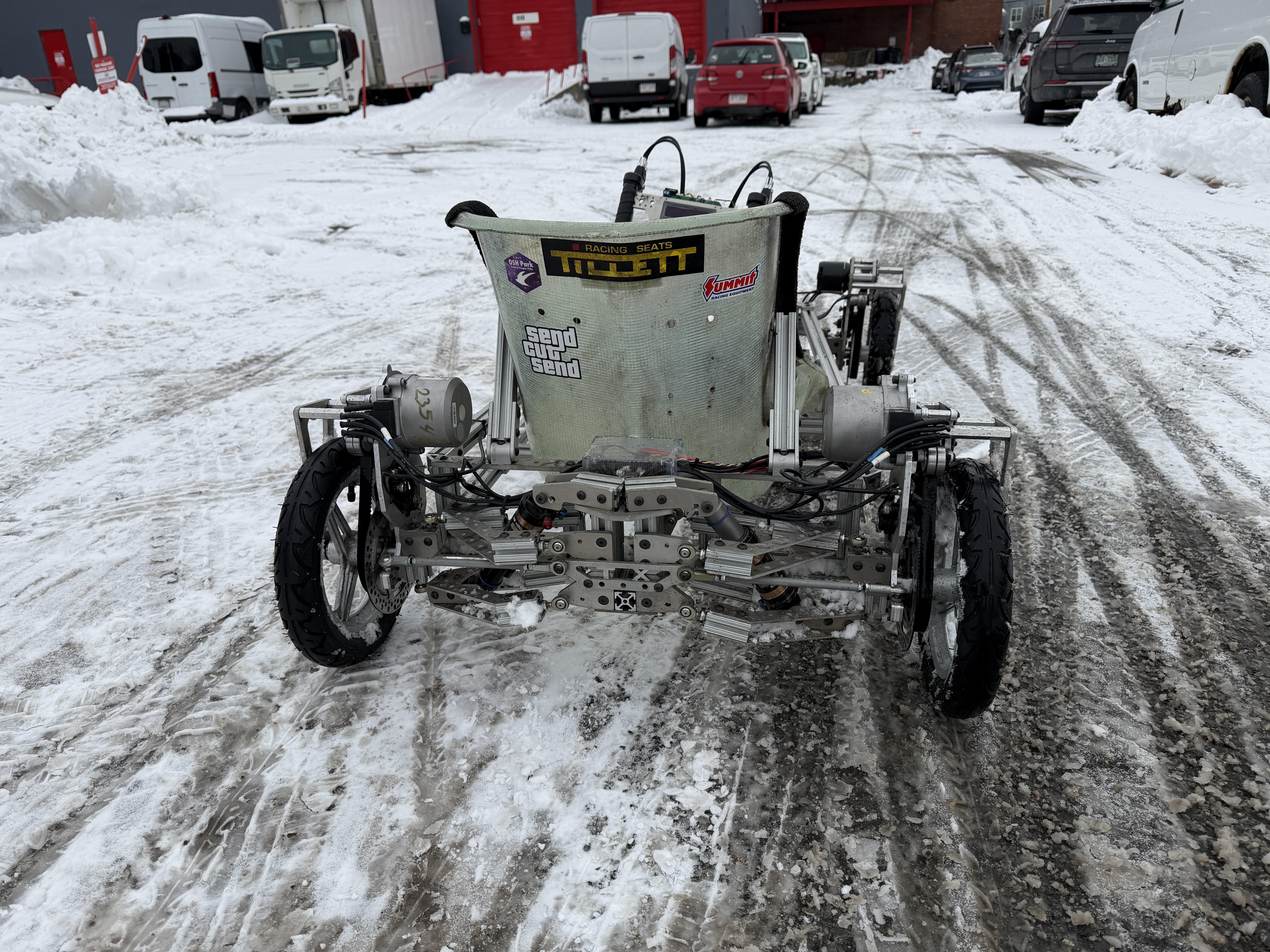
Earlier this year, I got to do some TinyCross ice racing on a frozen lake:
Thanks to Dane for organizing the event; there were over a dozen crazy ice vehicles. TinyCross wasn't the fastest, but the combination of four-wheel-drive, independent suspension, and traction control really helped it get off the line quickly and pull itself through ruts left in the slushy top layer by other vehicles. Overall, even though I didn't consider ice as a potential surface when designing this kart, it is surprisingly well-suited for it.
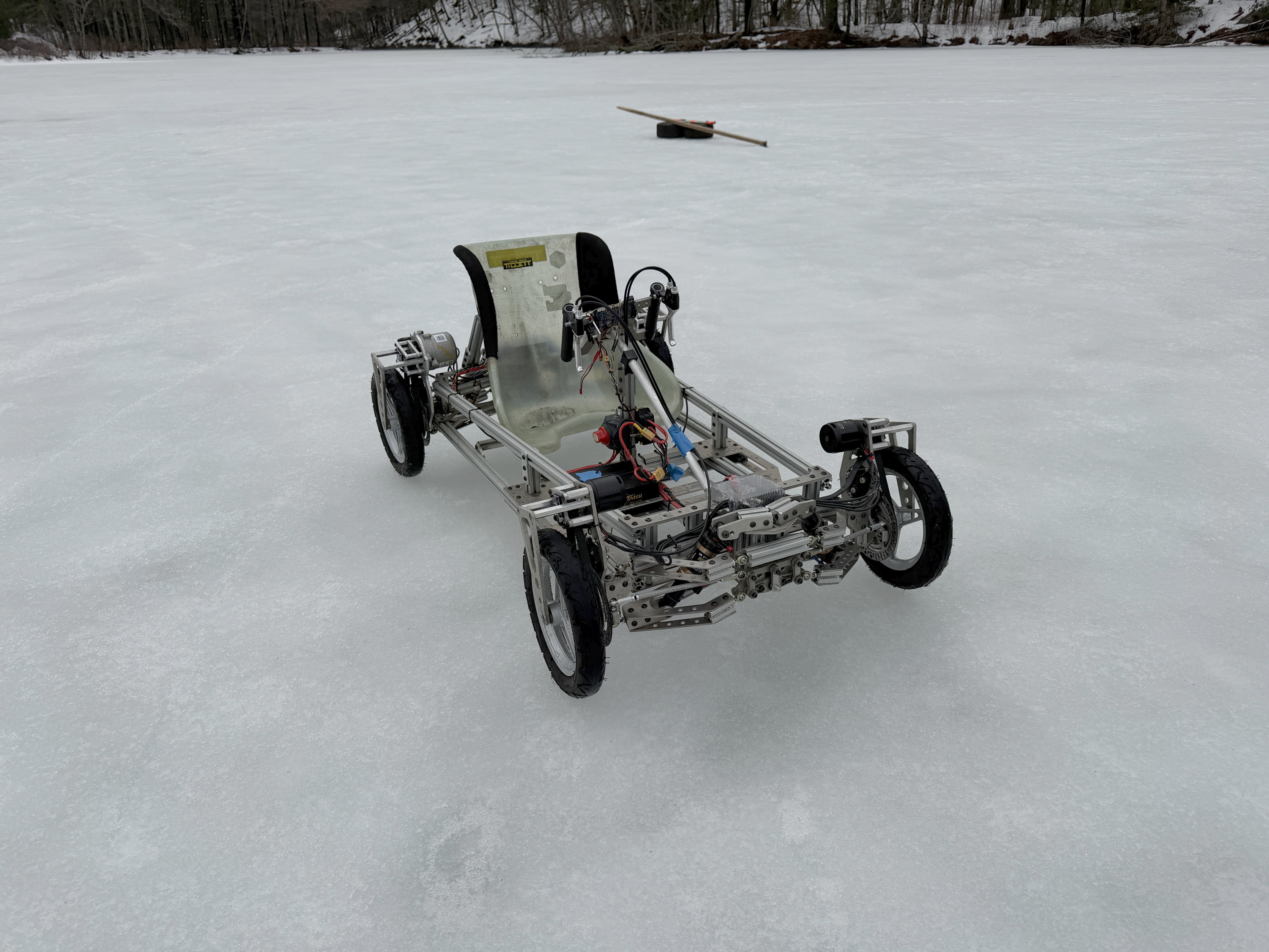
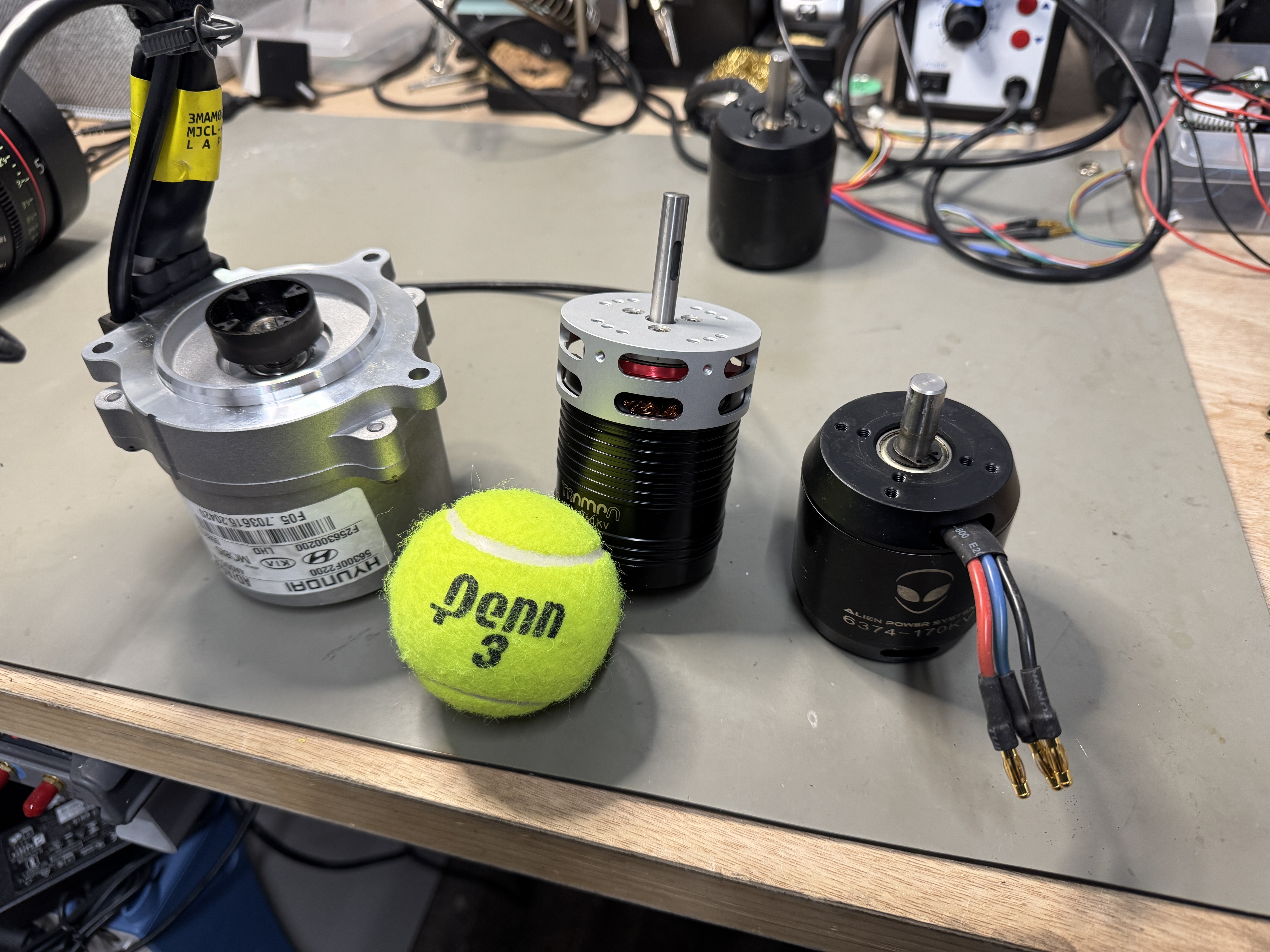
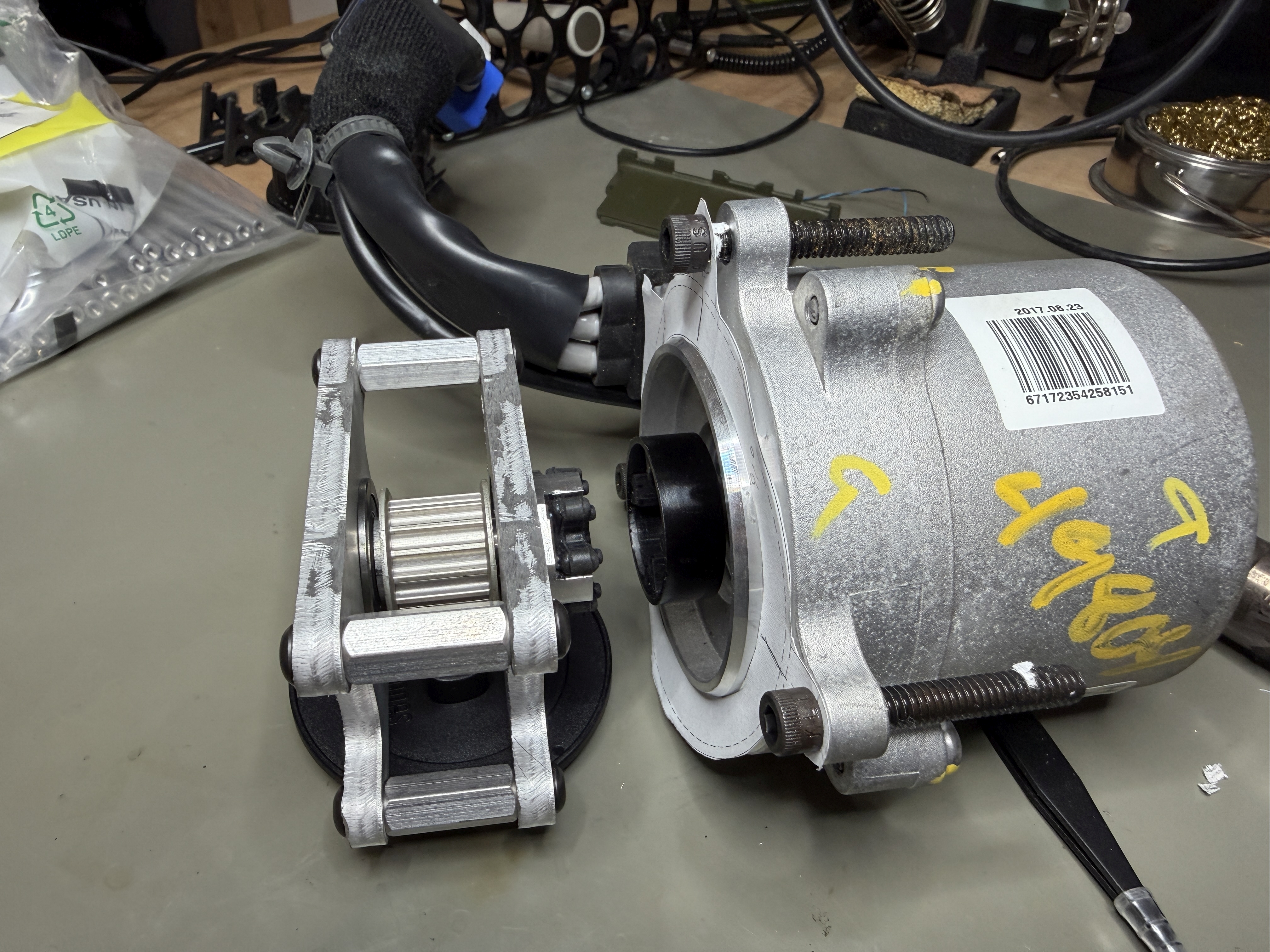
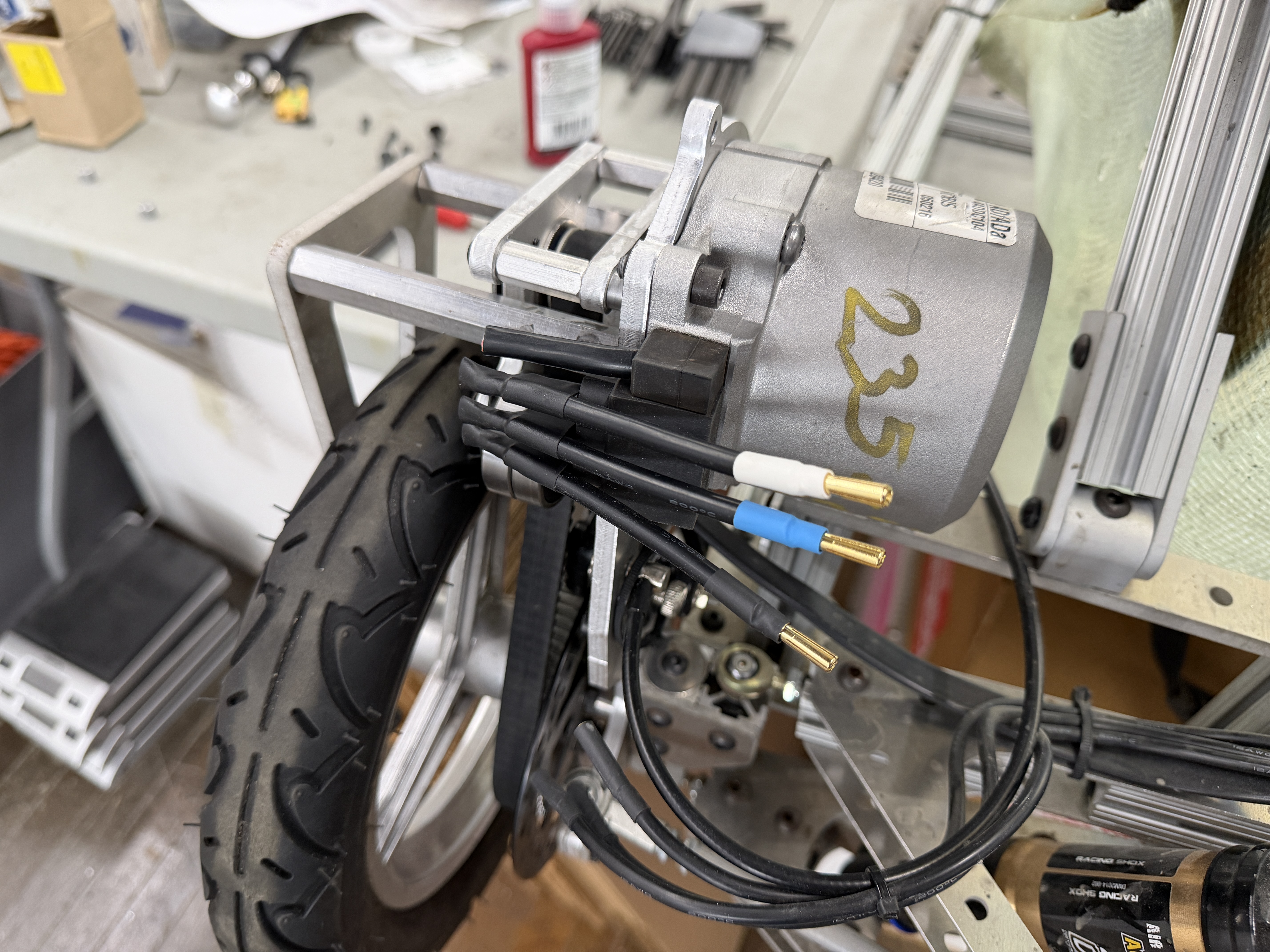
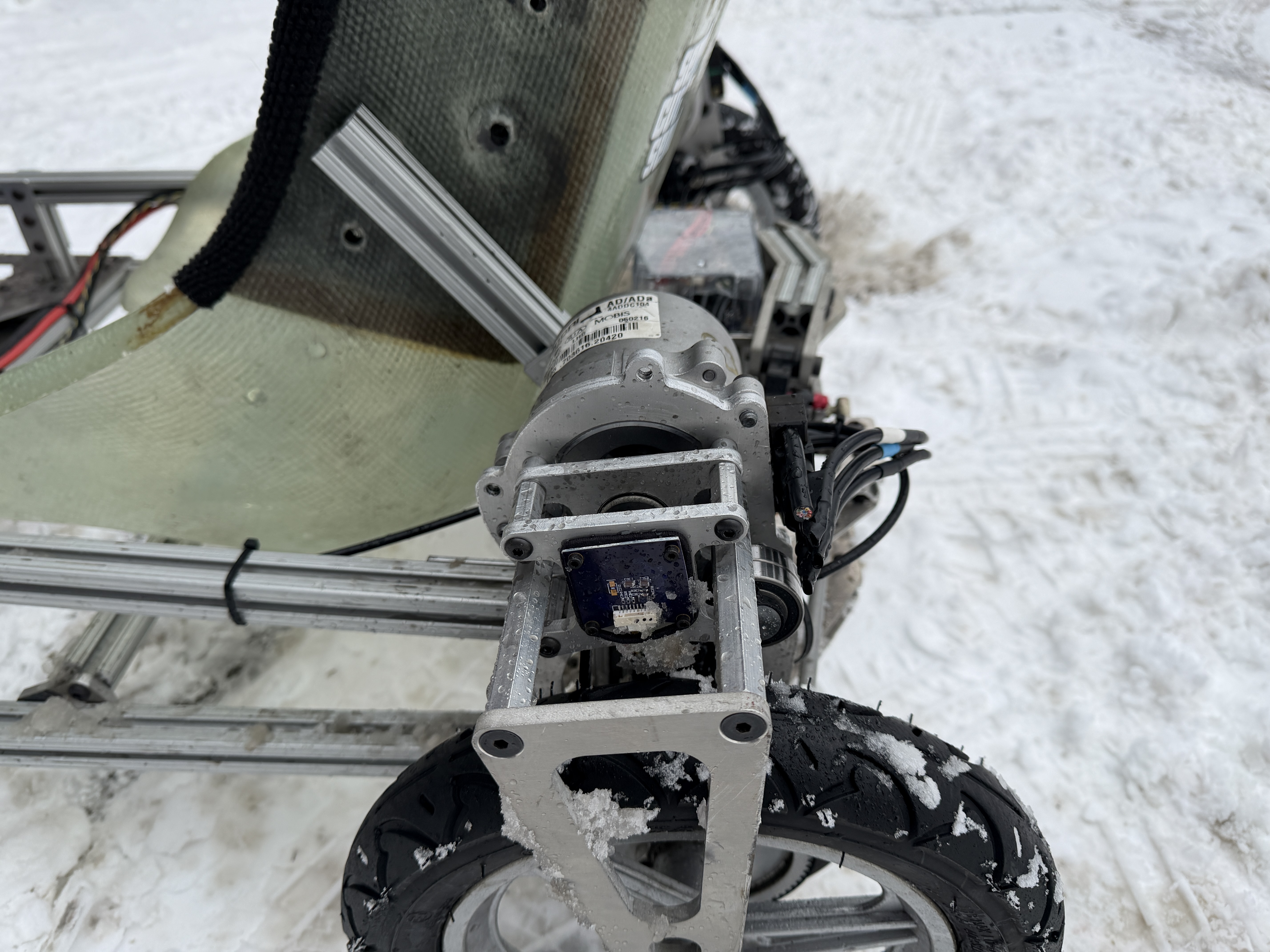
I participated last year, too, but after a couple runs, one of the rear motors was defeated by the slush. Either its position sensor failed (due to exposure to the elements, no doubt!) and caused it to lose sync, or another motor's sensor failed and the remaining one had to take up all the torque. Either way, the winding insulation melted quickly - the APS 6374-170KV motors can handle 100A peak, but not continuous. This was the main motivation for the rear motor swap, and I'm happy to report that the new Hyundai electric power steering motors held up to the challenge nicely.
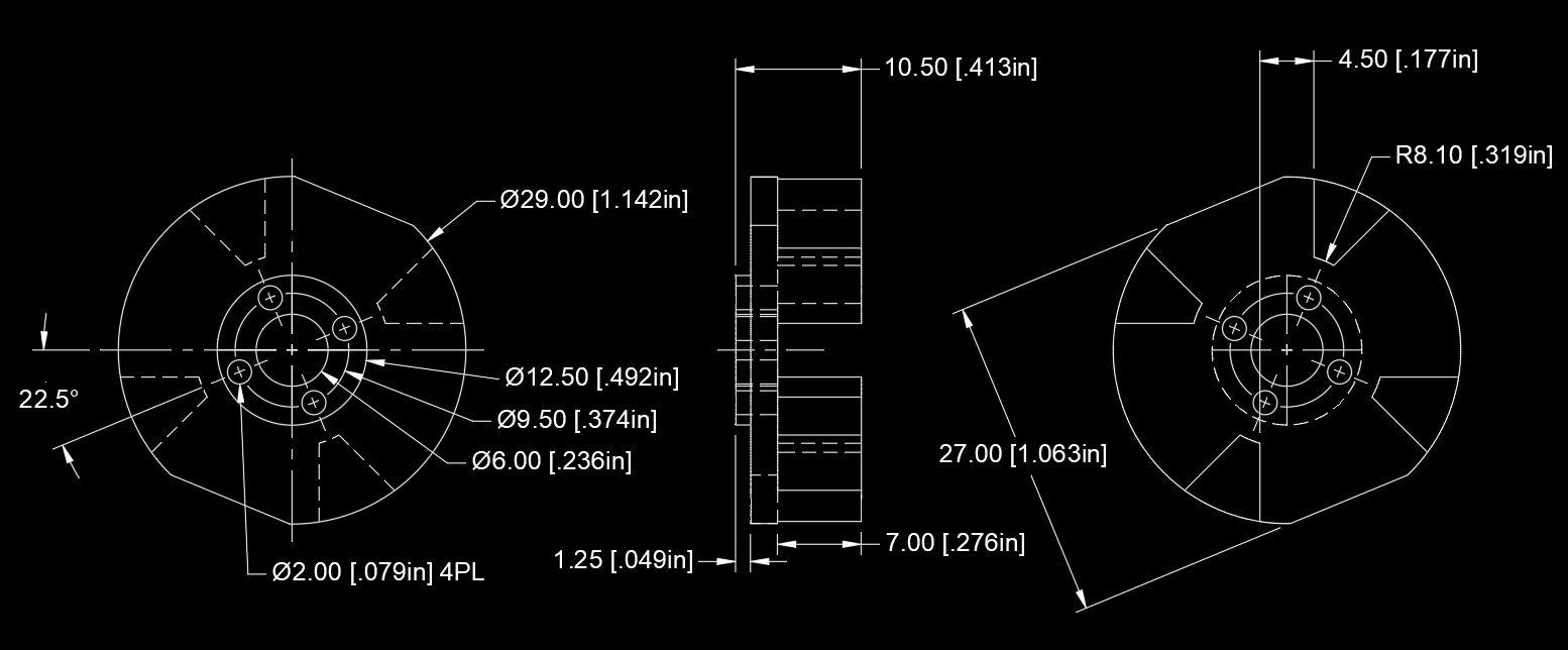
Hyundai 56300F2200 Motors
I've been able to collect some more data on the Hyundai 56300F2200 electric power steering motors that I swapped onto the rear wheels. They are, in fact, very close to the same torque/speed constant as the APS 6374-170KV:

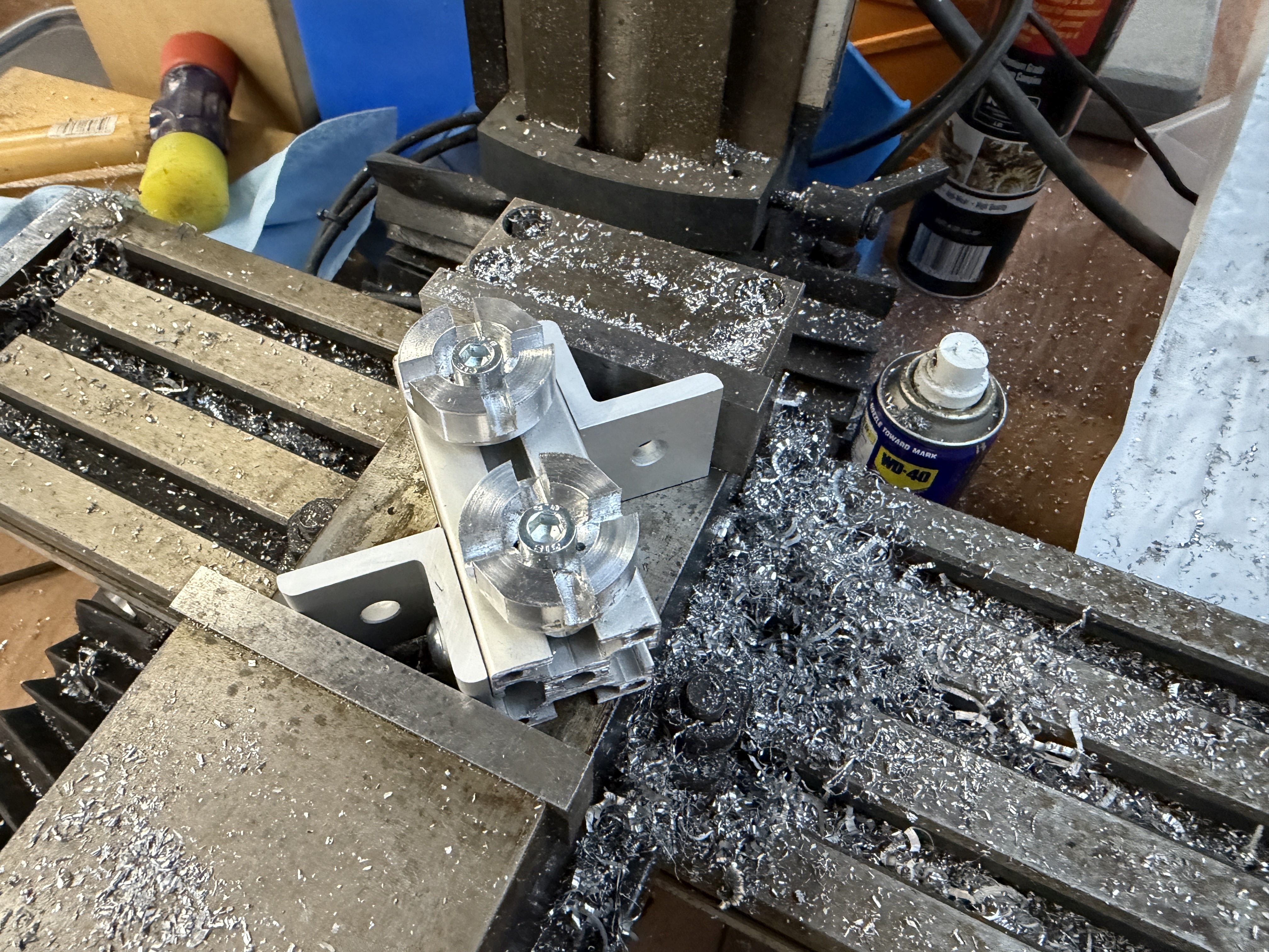
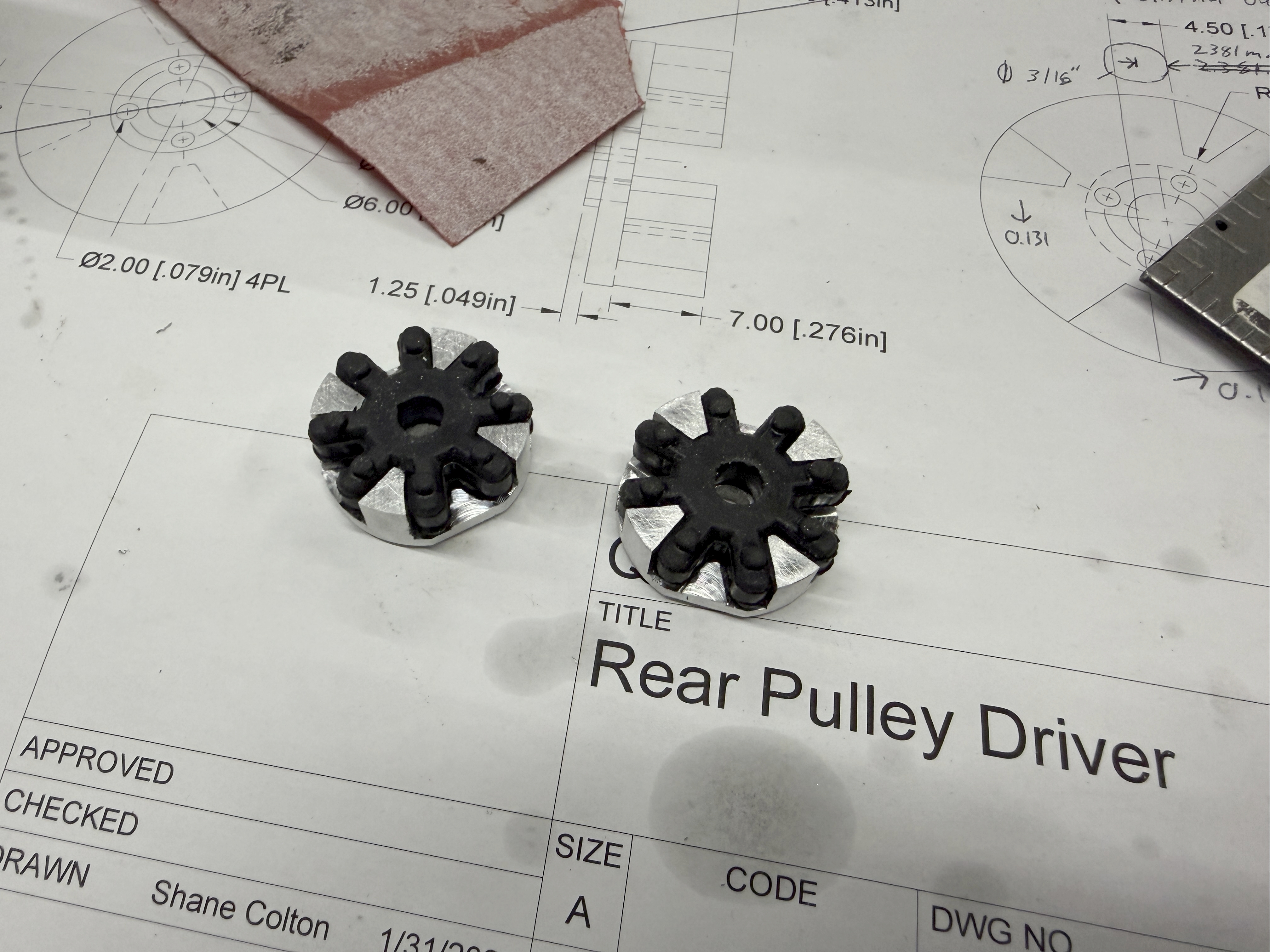
This is excellent, since I can keep the same gear ratio (70:15) and expect the same torque per amp and speed per volt, just with a much lower phase resistance. The line-to-neutral resistance on the Hyundai 56300F2200 is around 11mΩ, vs. about 27mΩ for the APS6374-170KV. The lower power dissipation, combined with the extra thermal mass and more direct cooling path of the inrunner configuraiton, means these motors can handle a lot higher peak and sustained current. The penalty, of course, is the extra weight.
I was initially worried about the inductance of the new motors, since they're designed for a 12V automotive system and I'm driving them at 48V. The synchronous inductance definitely is higher, at 120μH, vs. 50μH for the APS6374-170KV:

But, because they are only 6 poles instead of 14 poles, the lower electrical frequency almost exactly cancels the higher inductance in terms of how much D-axis voltage is required for a given mechanical RPM. It does still limit the maximum power, since the D-axis component of the voltage causes the total voltage to reach saturation much earlier than the back EMF alone would. Here's an example power curve with a maximum drive current of 100A (phase current) and drive voltage of 24V (line-to-neutral):

Using more current can generate more torque/force at low speeds, but causes the D-axis voltage to grow faster with frequency, so the peak power moves to lower speed:

Ultimately, the total impedance of the motor is what matters, and at high speed and high current, the reactive component becomes dominant. More voltage (for example with third harmonic injection) would help push to higher peak power. I also think the kart's always been geared a little hot for a 170rpm/V motor, so a slightly higher gear ratio could balance out the torque vs. speed a little better, if I can find the right pulleys.
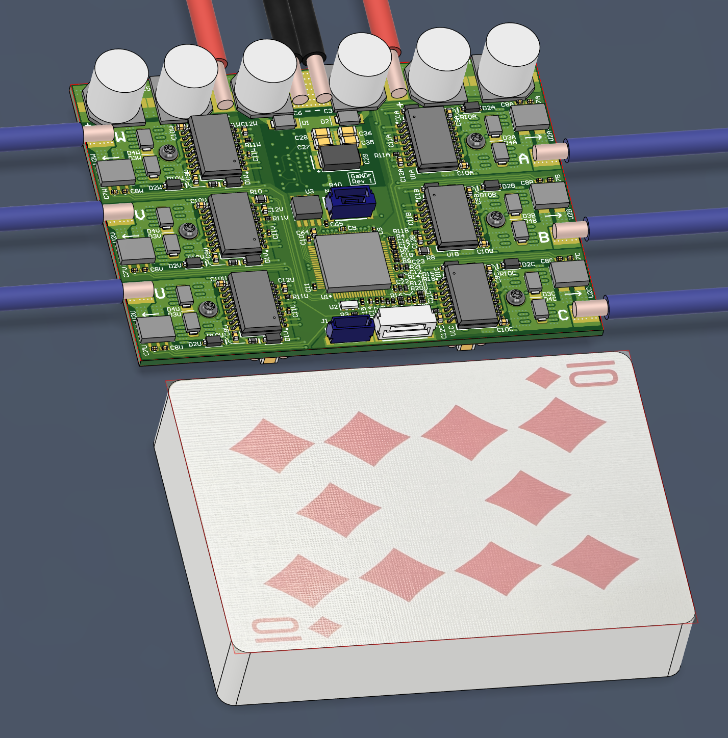
GaN Motor Drives
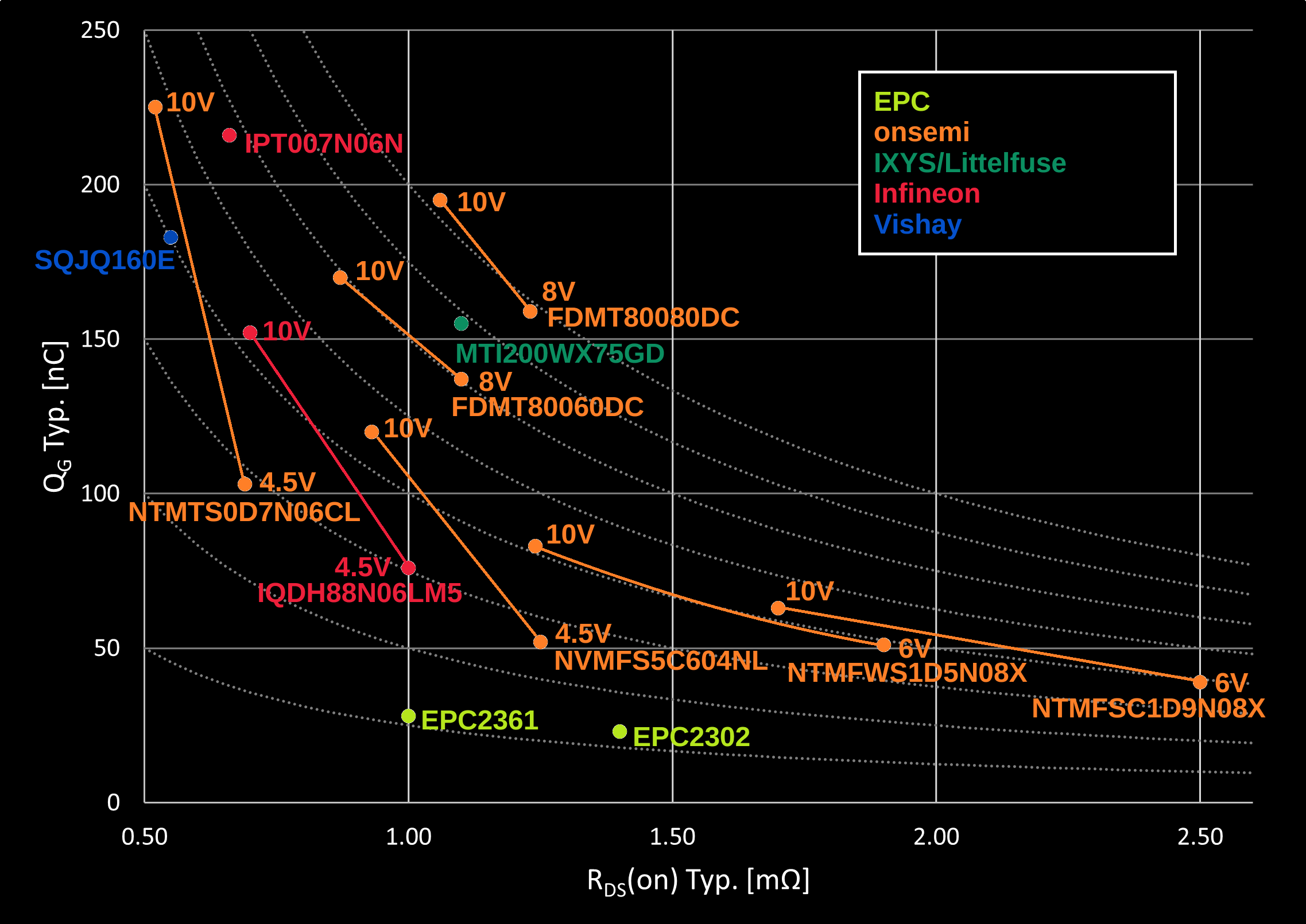
One other casualty of the rear motor swap has been any progress on my GaN FET motor drives. They were designed around the APS 6374-170KV motors, with a peak current of around 100A. The Hyundai 56300F2200 motors can handle more than that, so I'm not sure if the 2x EPC2302 per phase leg has enough margin anymore. Luckily, it's taken me so long to complete the project that the EPC2361 is also available now. EPC has a dev kit with two EPC2361 in parallel per leg specified for up to 184A peak AC current, so I feel somewhat confident in shooting for 150A in my design.
The new motors might also conflict with of the other main goals of the GaN drive project, which was to explore High-Frequency Injection (HFI) methods for sensorless start-up. The Hyundai motors seem to be surface permanent magnet inrunners with distributed windings, so they have barely any saliency. With an LCR meter, I only see a swing from about 116μH to 131μH, compared to 36μH to 63μH for the APS 6374-170KV. Pulling any rotor position information out of such a small difference in inductance might be hard. But I'll still give it a try.
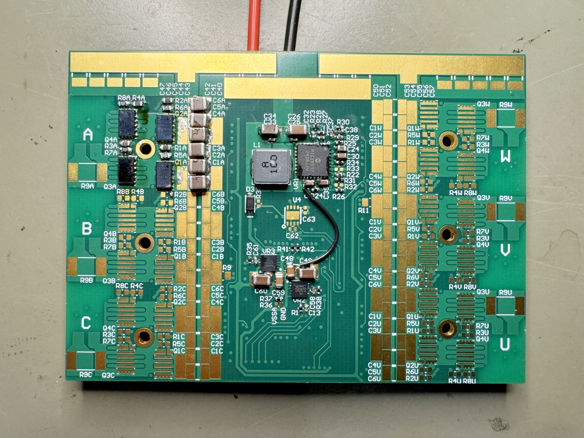
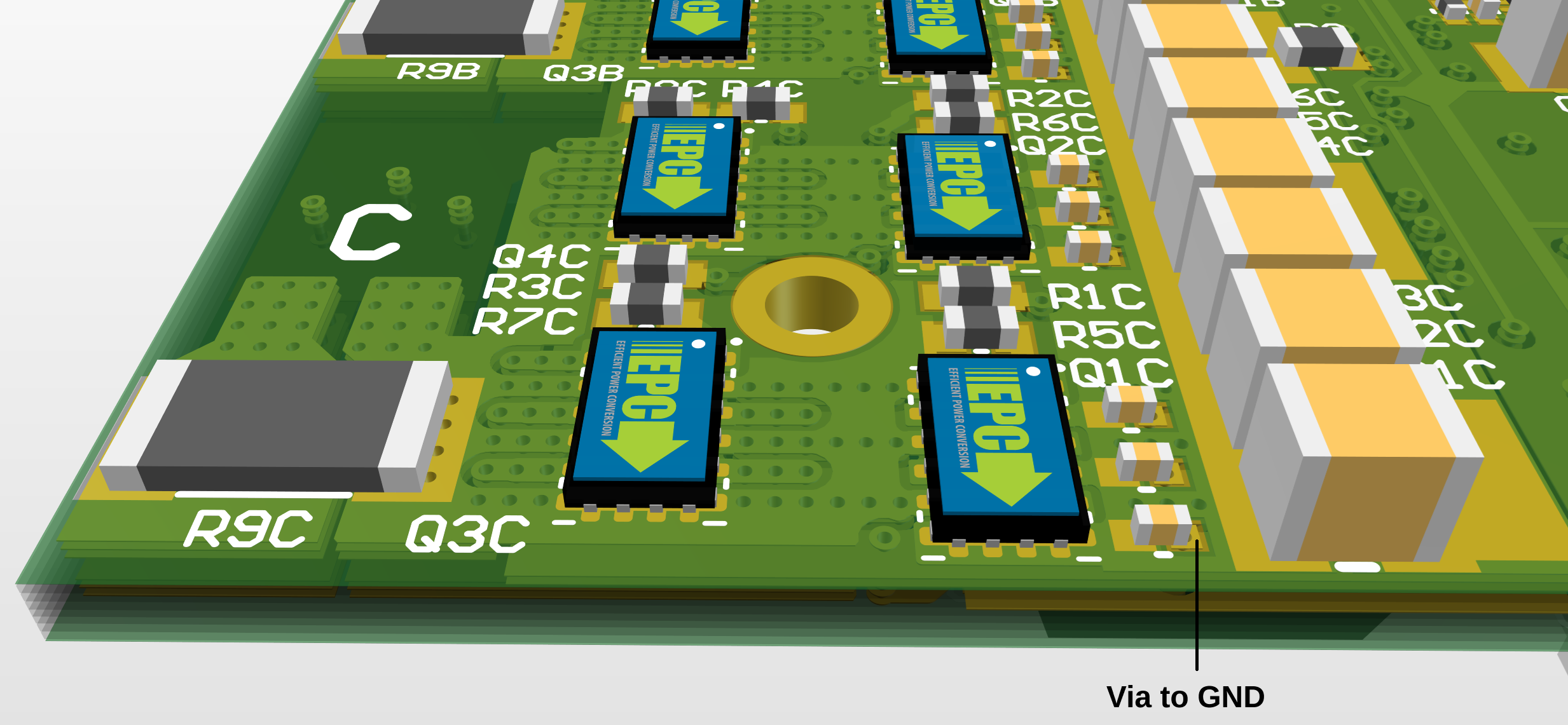
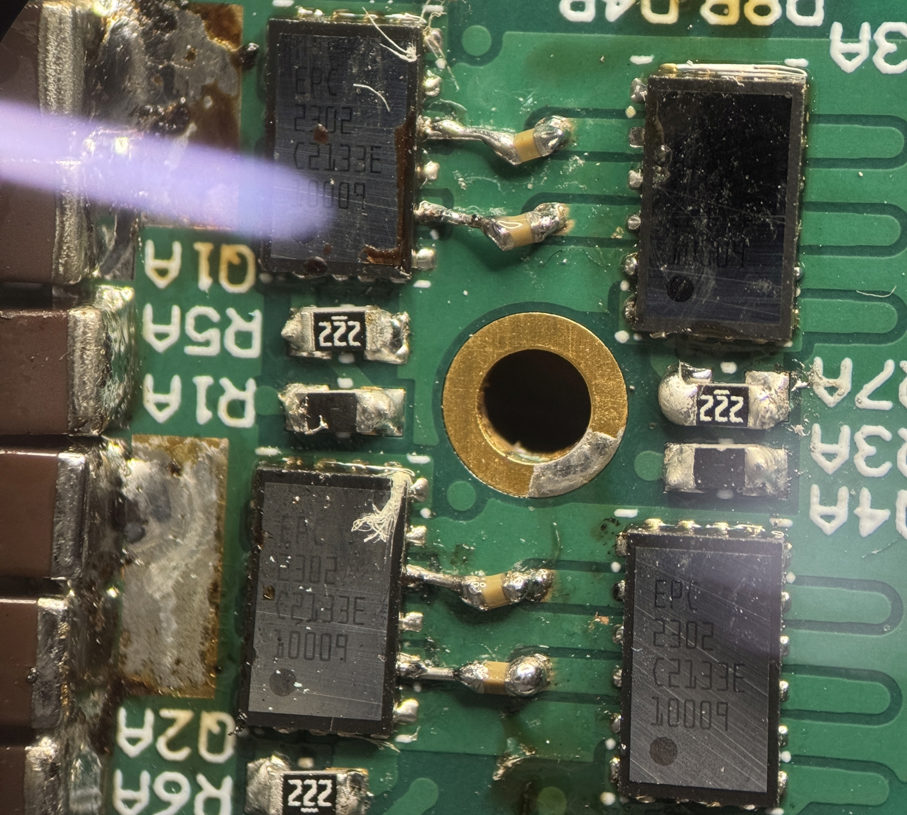
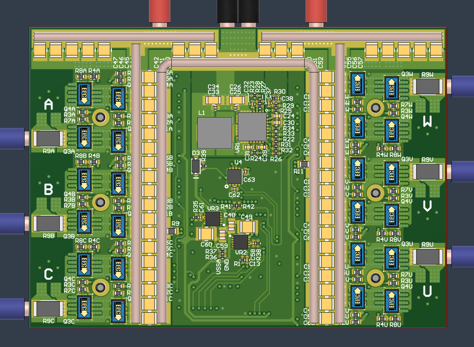
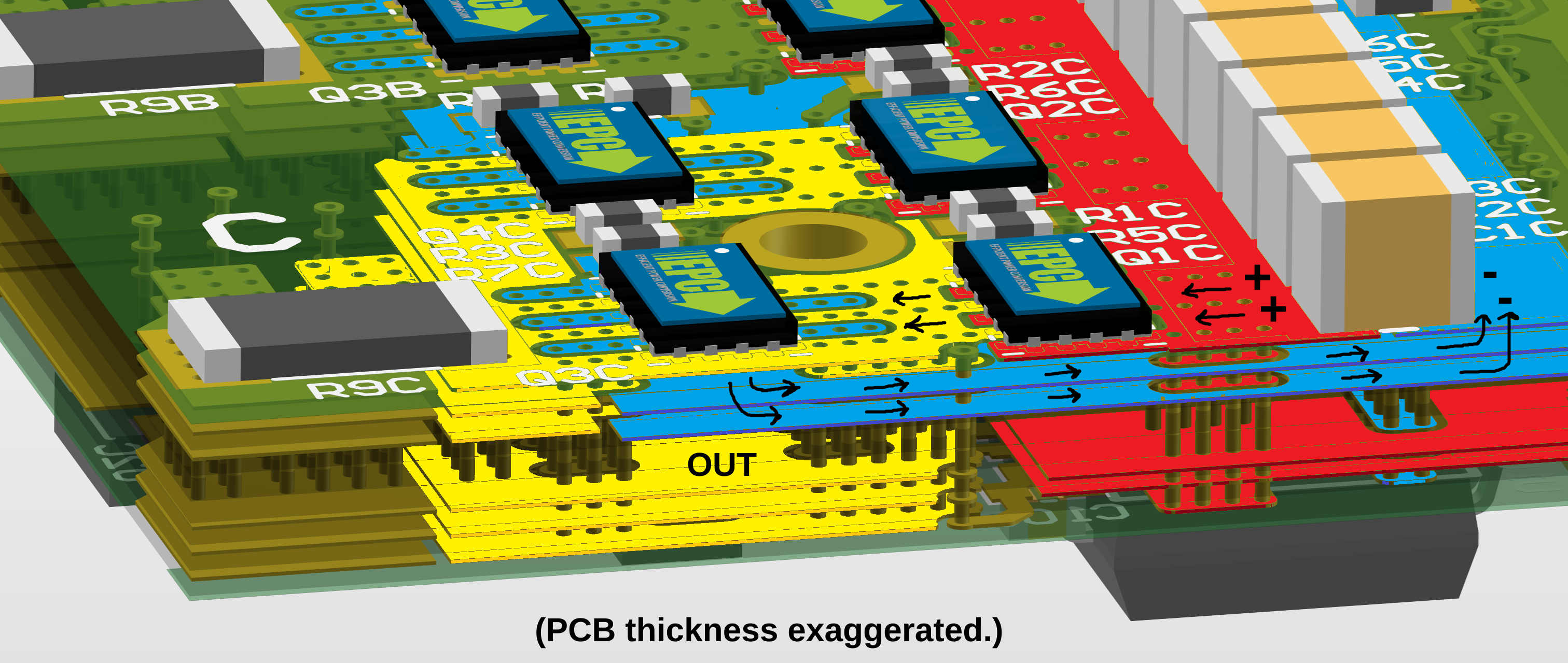
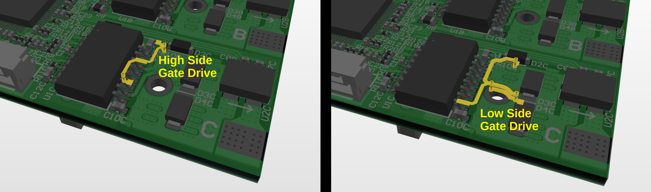
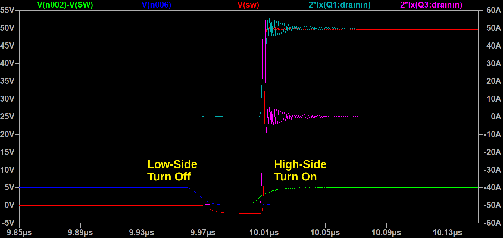
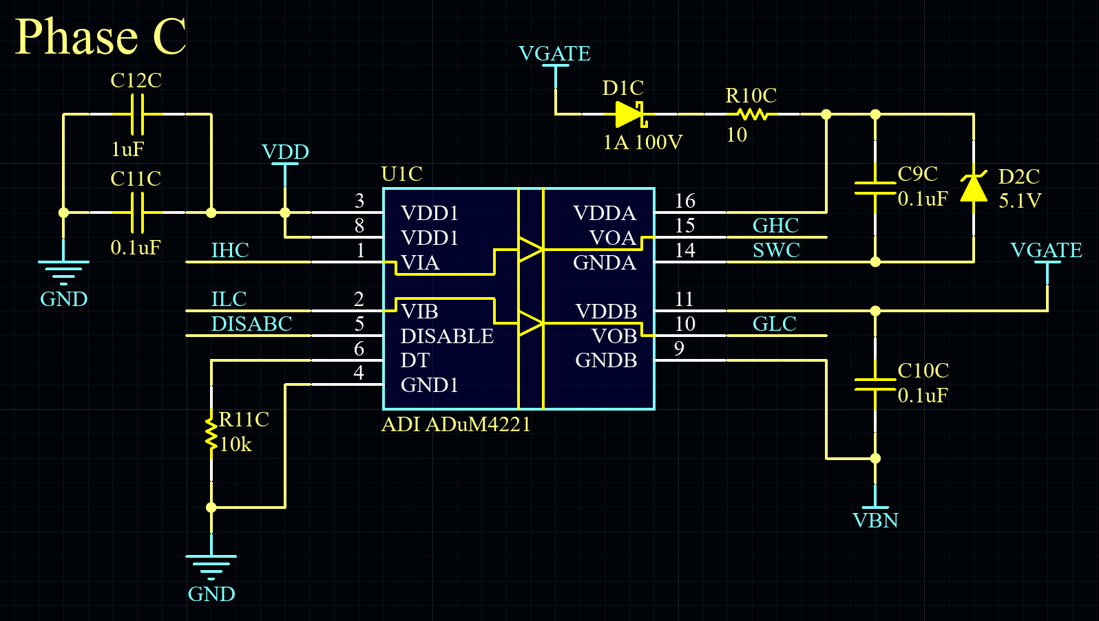
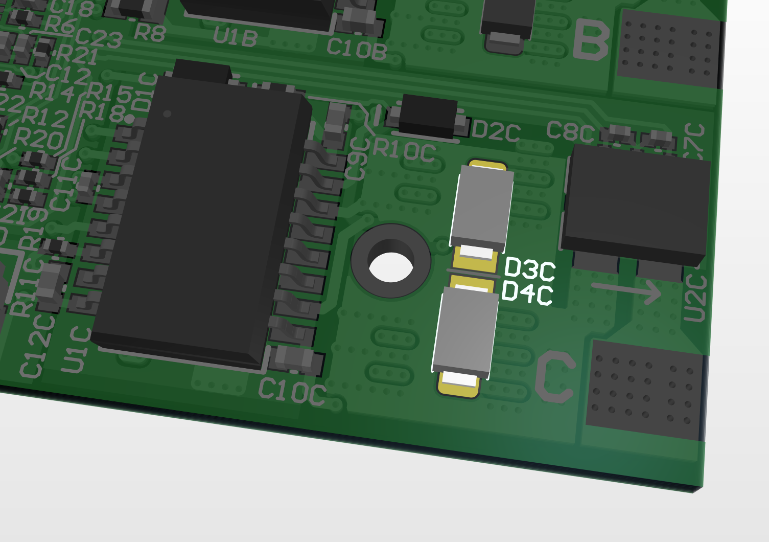
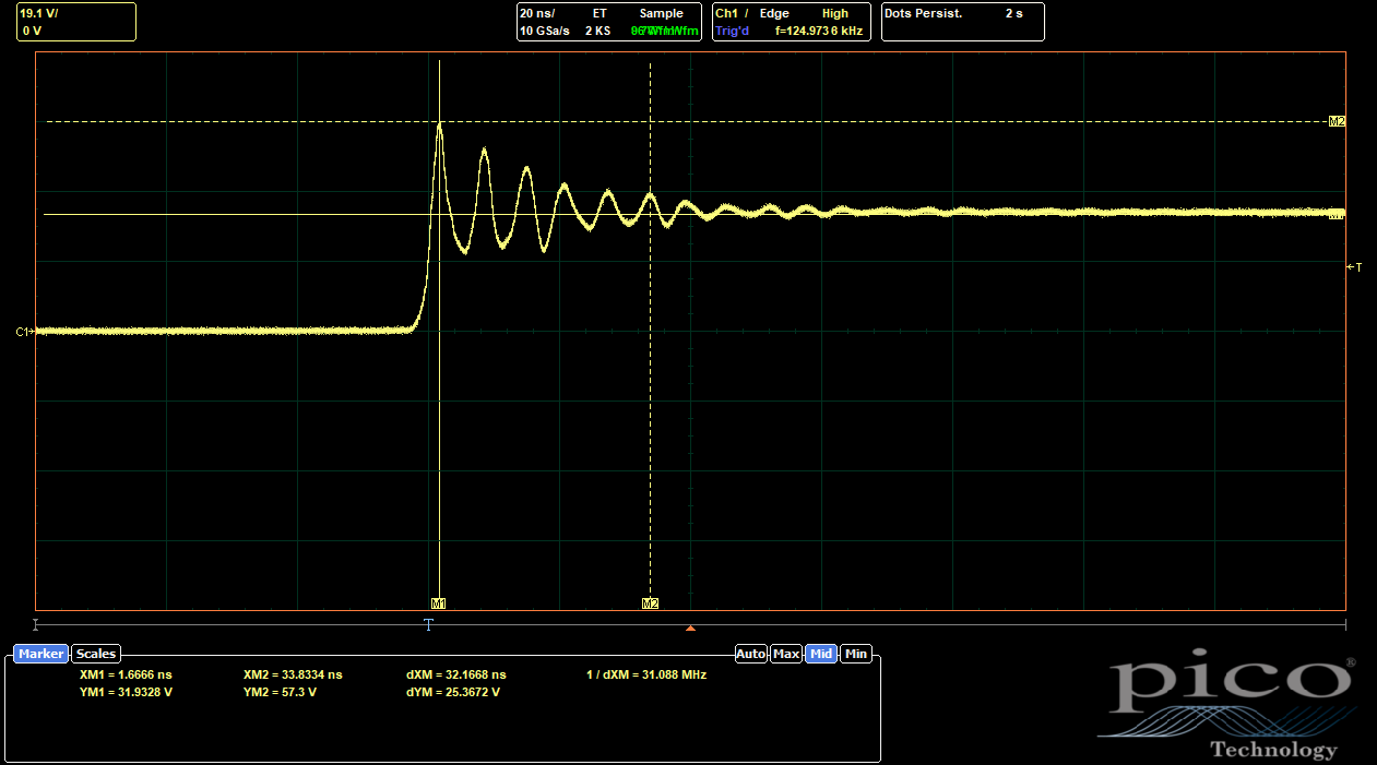
In the last GaNDr post, I proposed some layout modifications to improve the overshoot and ringing of the switch nodes on the GaN FET half-bridges. This ringing comes mostly from parasitic inductance in the PCB traces, so reducing the loop size as much as possible is key. Using small, fast MLCCs right near the FETs is important, even if you still need large bulk capacitance further out on the DC bus. To recap, there were two possible locations for adding some extra fast 0402 MLCCs:
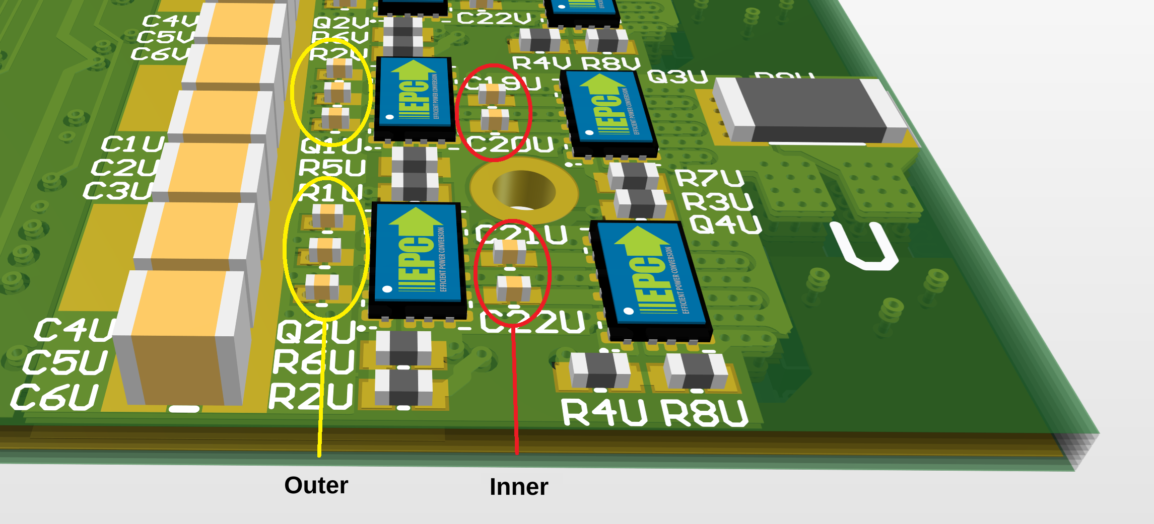
I routed the Rev 2 board with one side (ABC) using only the "outer" option and one side (UVW) using both options. (The "inner" caps were not guaranteed to be an improvement, in my view, since they might make the outer loop routing less ideal, so I wanted to test a version without the routing for those caps.) Here are the results from the ABC side:
 |
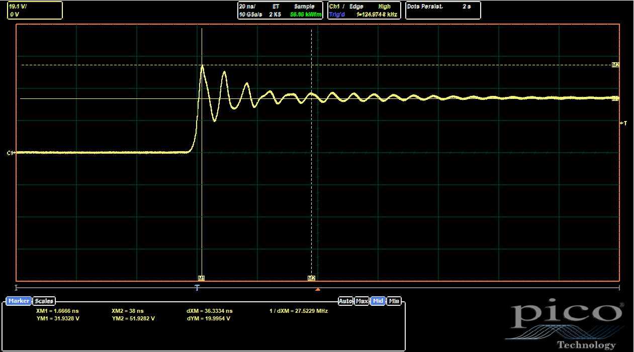
| ABC Side, Baseline (No 0402s Populated) |
 |
| ABC Side, Outer 0402s Populated |
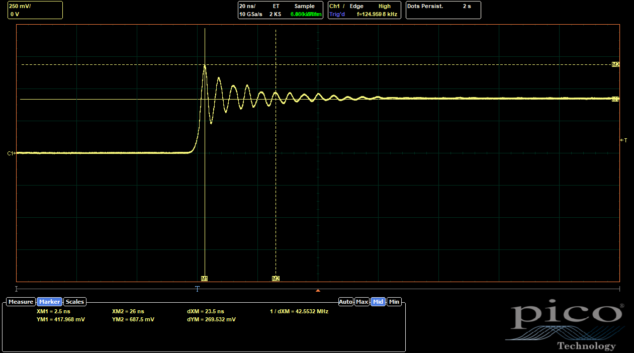
Adding the outer 0402s only reduced the overshoot from 80% to 74%, not as much as I would have expected. The ringing frequency does increase, which shows that the parasitic inductance has been reduced slightly. (The natural frequency of the parasitic circuit scales as (LC)-0.5, and C is mostly determined by the FETs.) But the effect wasn't as significant as I would have liked.
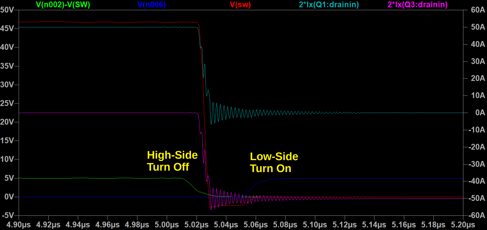
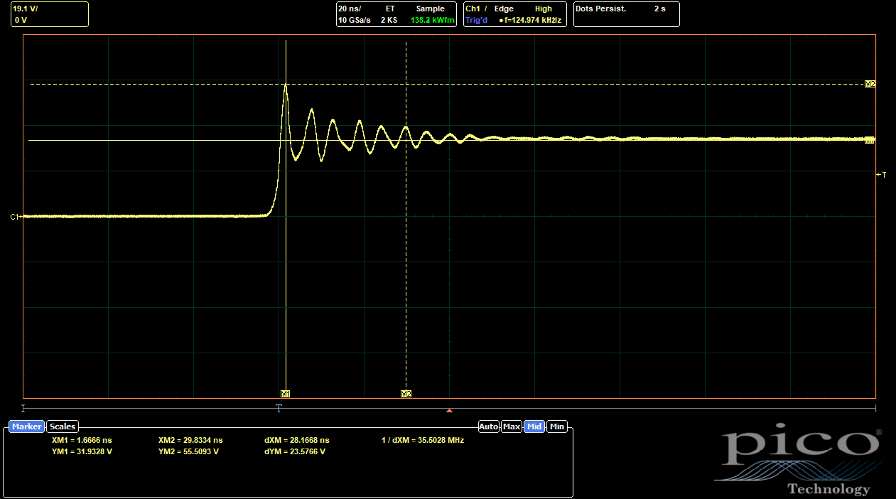
The UVW side, with both 0402 placements, is much more interesting:
 |
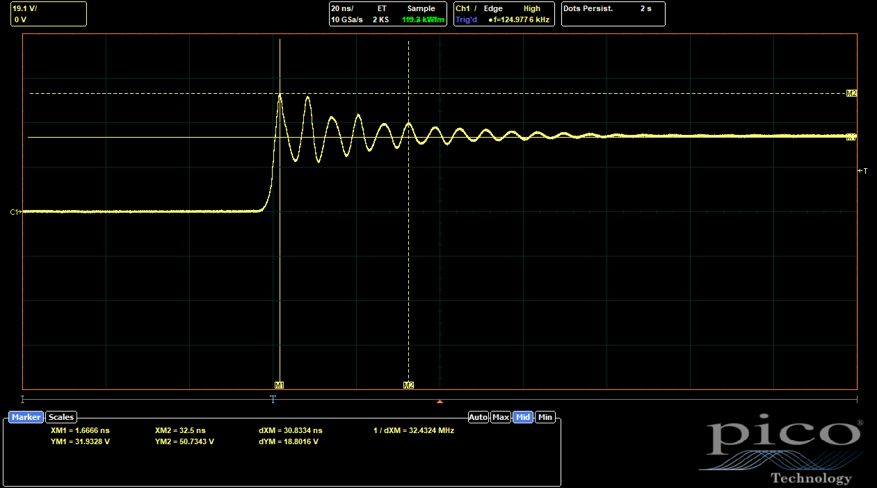
| UVW Side, Baseline ((No 0402s Populated) |
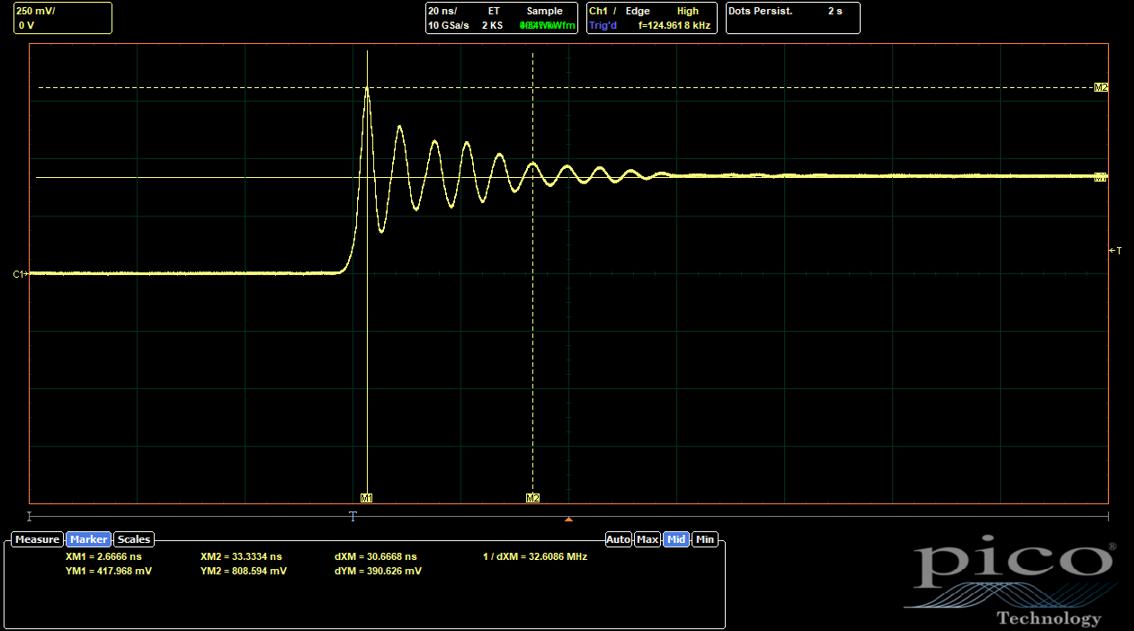
The baseline, without any of the 0402s placed, is already better than both ABC cases, at 63% overshoot. So I guess somehow the new routing is actually better? I don't really understand why, since it breaks up the L2 ground return path, which should be disadvantageous if not actually using the inner 0402s. But, the scope doesn't lie. Adding in the 0402s helps even further:
 |
| UVW Side, Only Outer 0402s Populated |
 |
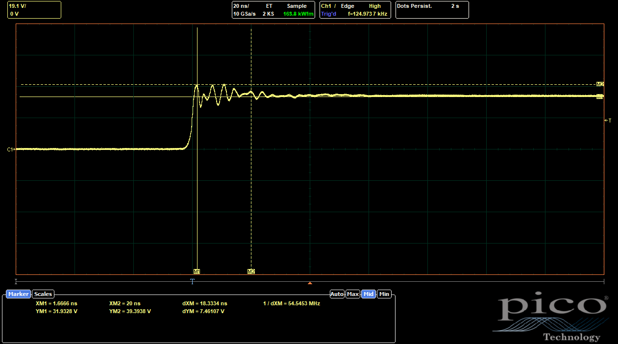
| UVW Side, Only Inner 0402s Populated |
 |
| UVW Side, Outer and Inner 0402s Populated |
The inner 0402s make a much more substantial difference than the outer ones. With only the outer 0402s, the overshoot is only reduced to 59%, a proportionally similar reduction from baseline compared to the ABC side. With only the inner 0402s, though, the overshoot comes all the way down to 27%. With both options populated, the combined effects only drop it a bit more, to 23%. So it's clear the inner 0402s are doing most of the work to reduce the parasitic inductance.
The ringing is no longer a single frequency, which suggests that the two current loops (one to the inner 0402s and one to the outer 0402s and/or the big 1210 DC bus caps) have different natural frequencies and are interfering with each other. But one of the frequencies (presumably the one associated with the lower-inductance inner 0402 path) seems to be considerably higher.
This is a pretty surprising result, since I haven't really seen any GaN layouts like this. It is mentioned in the EPC layout guidelines as an option, though, so it's not totally crazy. Based on these results, I will likely commit to the inner 0402s with the new layout and remove the outer 0402s entirely. The space was more useful for a DC rail busbar to help carry high current down the board to each of the phases, something that might be necessary now with the Hyundai motors.
Batteries
Next on my list of components to upgrade on TinyCross are the batteries. The Tattu Plus 10Ah packs have worked well, but I think I can do a little better with cylindrical 21700 lithium-ion cells these days. Here's the concept:
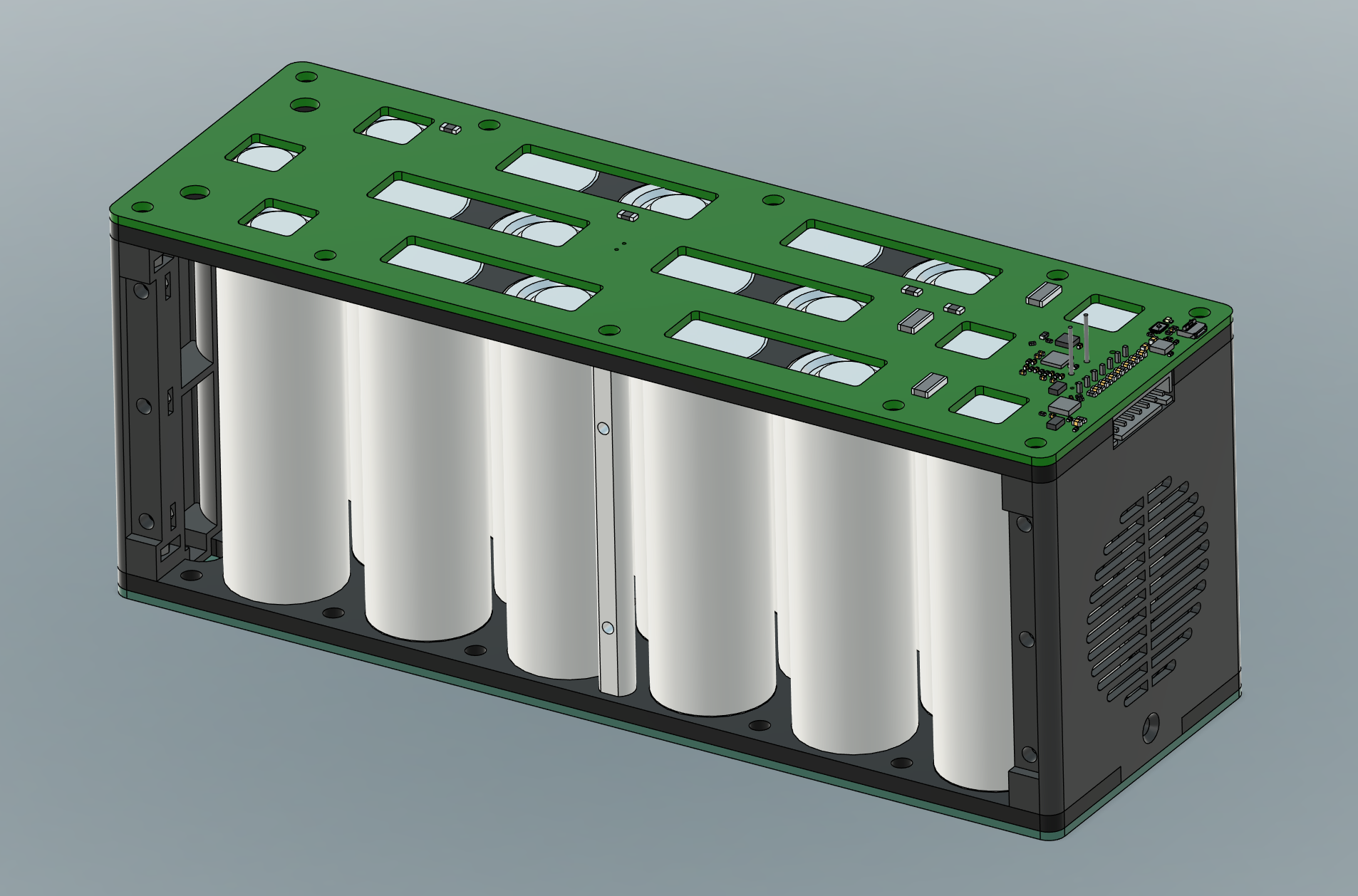
The cells are Molicel INR-21700-P50B, in a 6S3P configuration. This puts the total pack at 15Ah, a nice 50% gain in roughly the same volume as the current packs. These are considered power cells, with a 60A (12C) maximum discharge rating and a DCR of around 15mΩ. The Tattu Plus still has a slight edge on power, thanks to its 25C discharge rating, but these will work just fine for TinyCross. With two packs in series, I'll have 7.8kW available. And with the full load of four packs (2S2P at the pack level), I'll have 15.6kW. That's more than enough power, and the extra capacity is more useful.
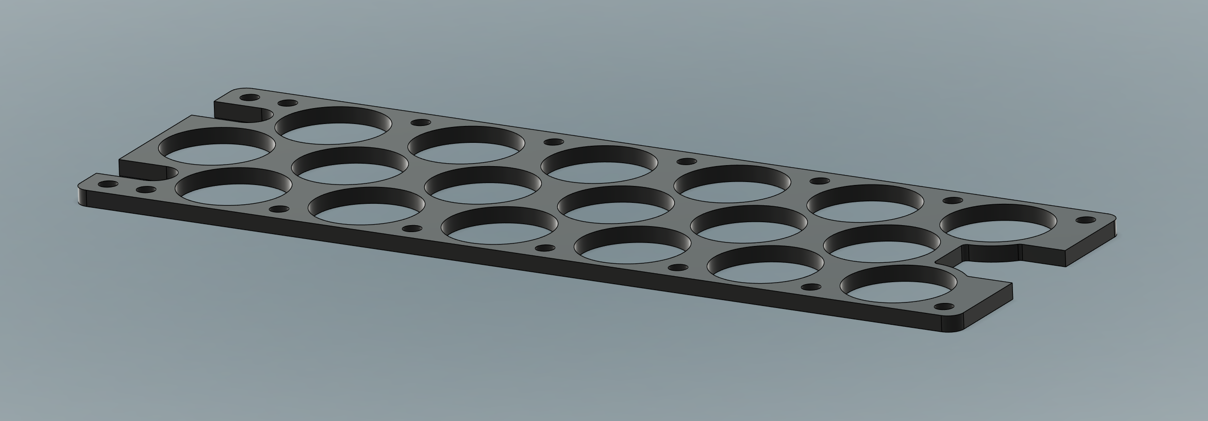
Matching the form-factor of the existing packs is convenient, since I can use the same mounting slots on the kart. The cells arrange conveniently in that shape. To hold them together, I have two laser-cut Delrin spacers separated by 2.5in standoffs. Sandwiching this are two PCBs: a bottom one just used to collect up some cell monitoring voltages, and a top one with the BMS. Both PCBs have slots for nickel tabs, which carry most of the current down the series strings. In order for both leads to come out on the same side of the pack, current returns from the end of the strings on two inner layers of 2oz copper:
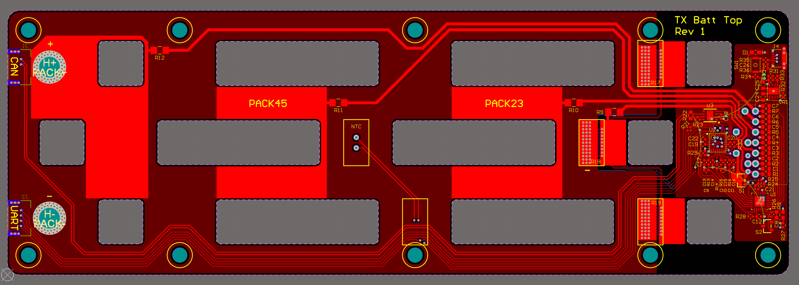
The BMS consists of a TI BQ76925 analog front end paired with an STM32F0 microcontroller, all crammed into one side of the top PCB. It can monitor individual cell voltages, pack current, and temperature (via a thermistor in the middle of the pack). It also can do resistive cell balancing, although I've included the standard 7-pin JST XH header for external balancing anyway. I still plan to use a dual-channel RC-style charger to charge the packs, so I'm not including any cutoff FETs. However, the STM32F0 can talk to other packs via isolated UART and to the rest of the kart via CAN.
The two end caps are 3D-printed (Nylon, SLS) and the sides, top, and bottom will probably get thin polycarbonate sheets, if I don't get lazy and put the whole thing in some big heat shrink instead. Thinking ahead to next year's ice racing, I've also left a spot for a power resistor and fan, to hopefully push some warm air through the gaps between the cells.
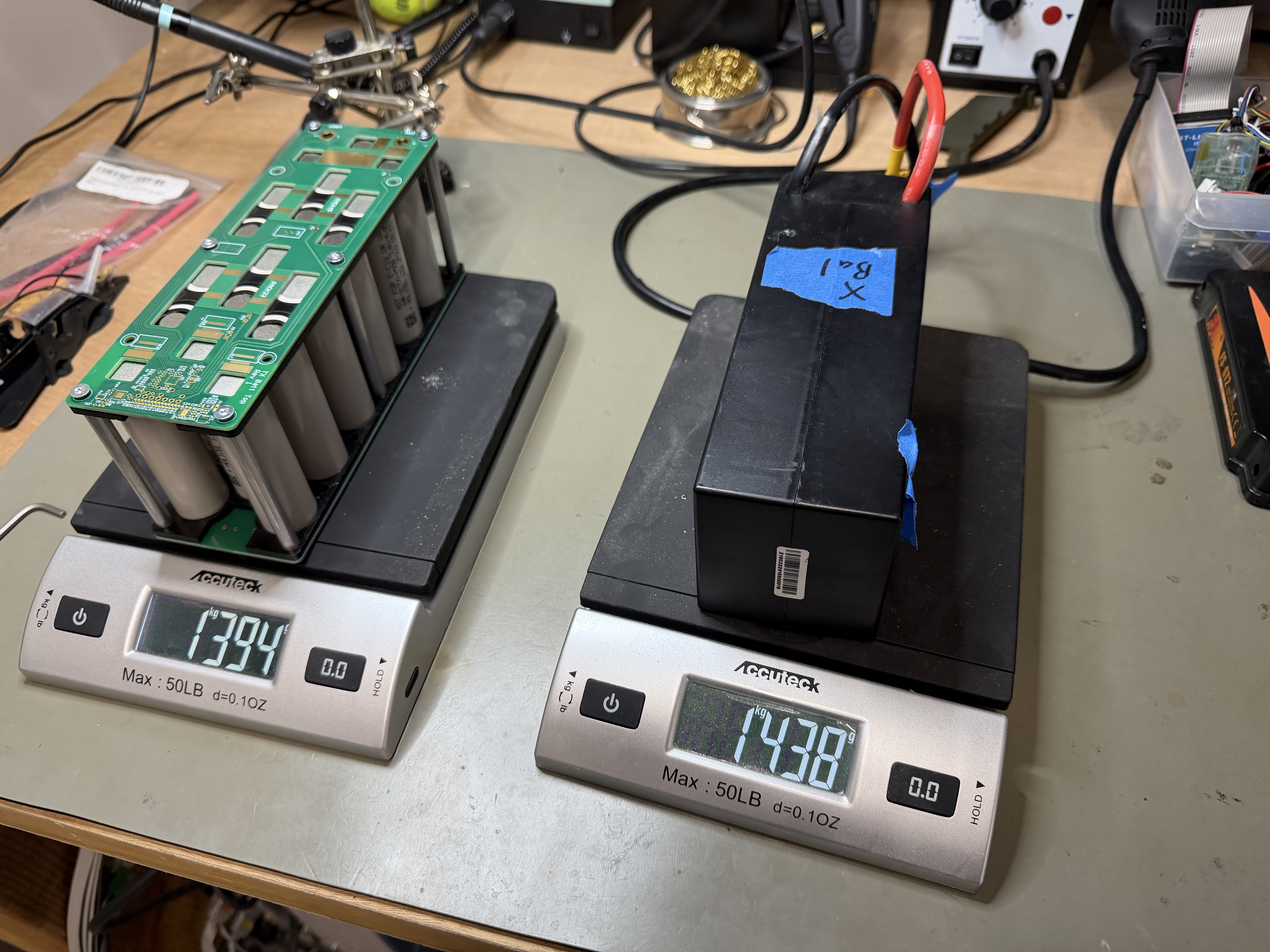
The cells, spacers, and PCBs together weigh a bit less than the Tattu Plus 10Ah packs, but I expect once I add the nickel tabs, wires, and all the end caps and side panels, they'll be slightly heavier, maybe around 1.5kg each. But, at 15Ah, the energy density will be much higher. I'm going through the BMS bring up slowly; there's no rush to get these done since I still have the Tattu packs. Also, the kart is currently inoperable for other reasons...
Mechanical Upgrades?
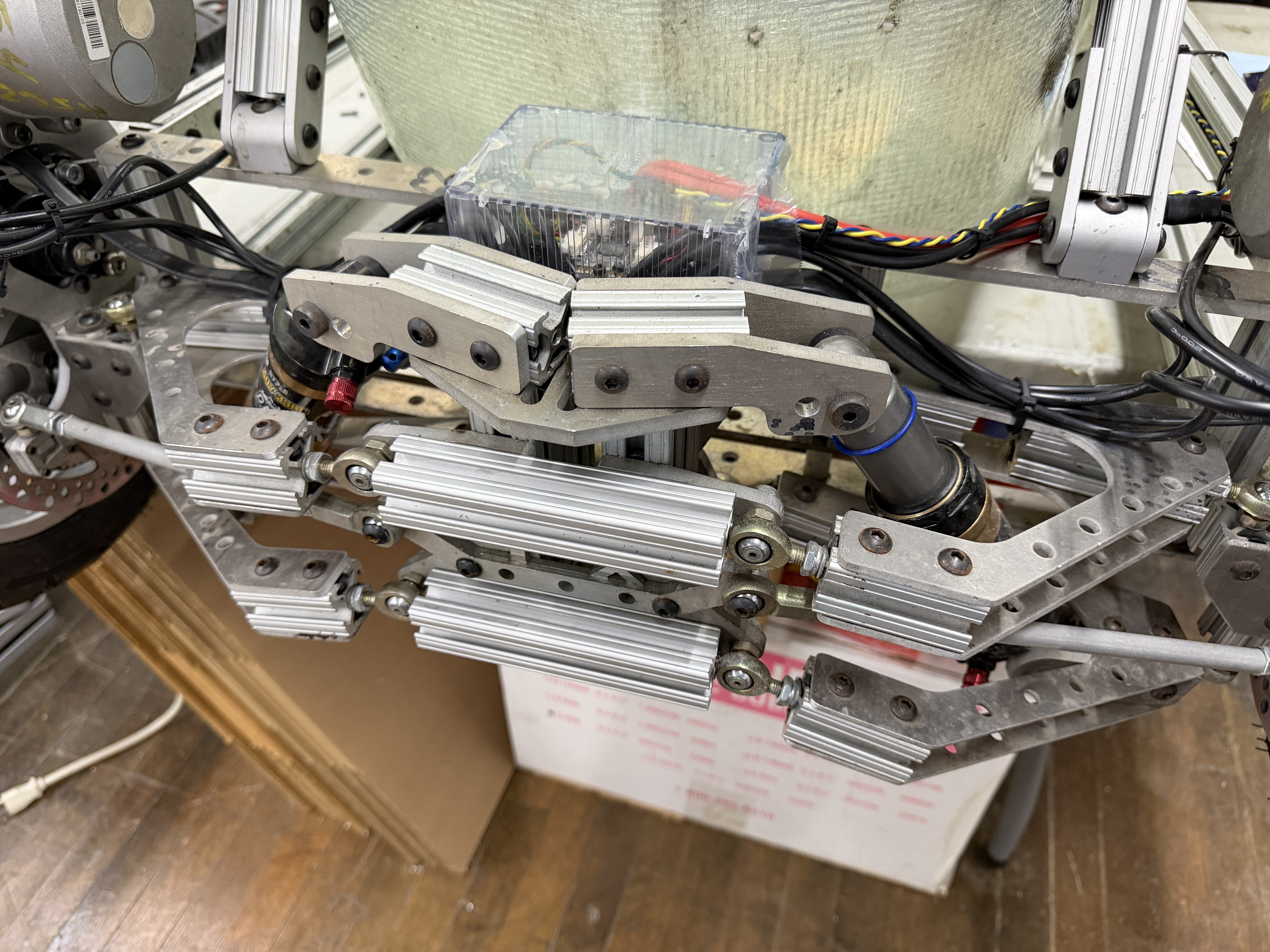
During a non-icy test run with the new motors, this happened:
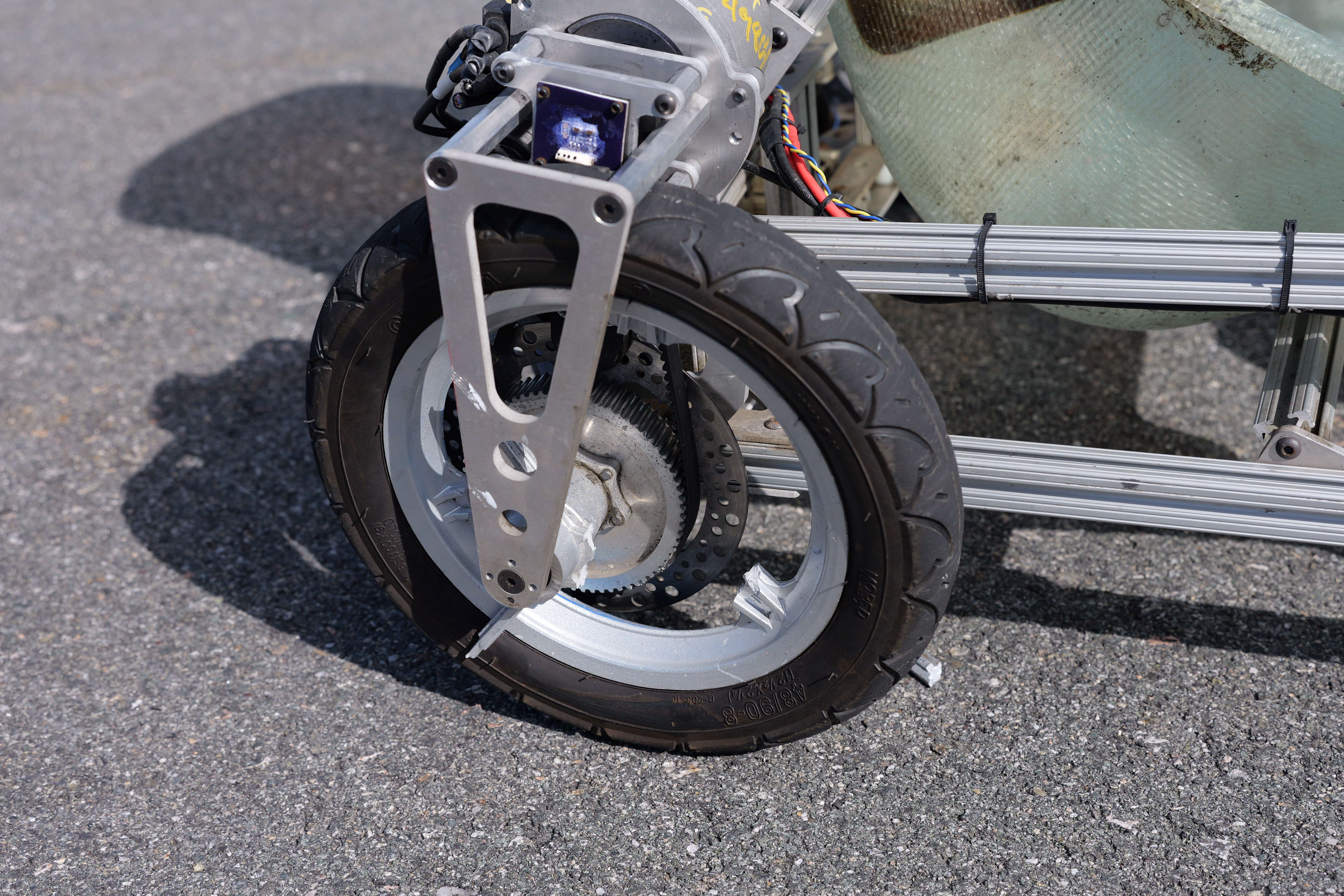
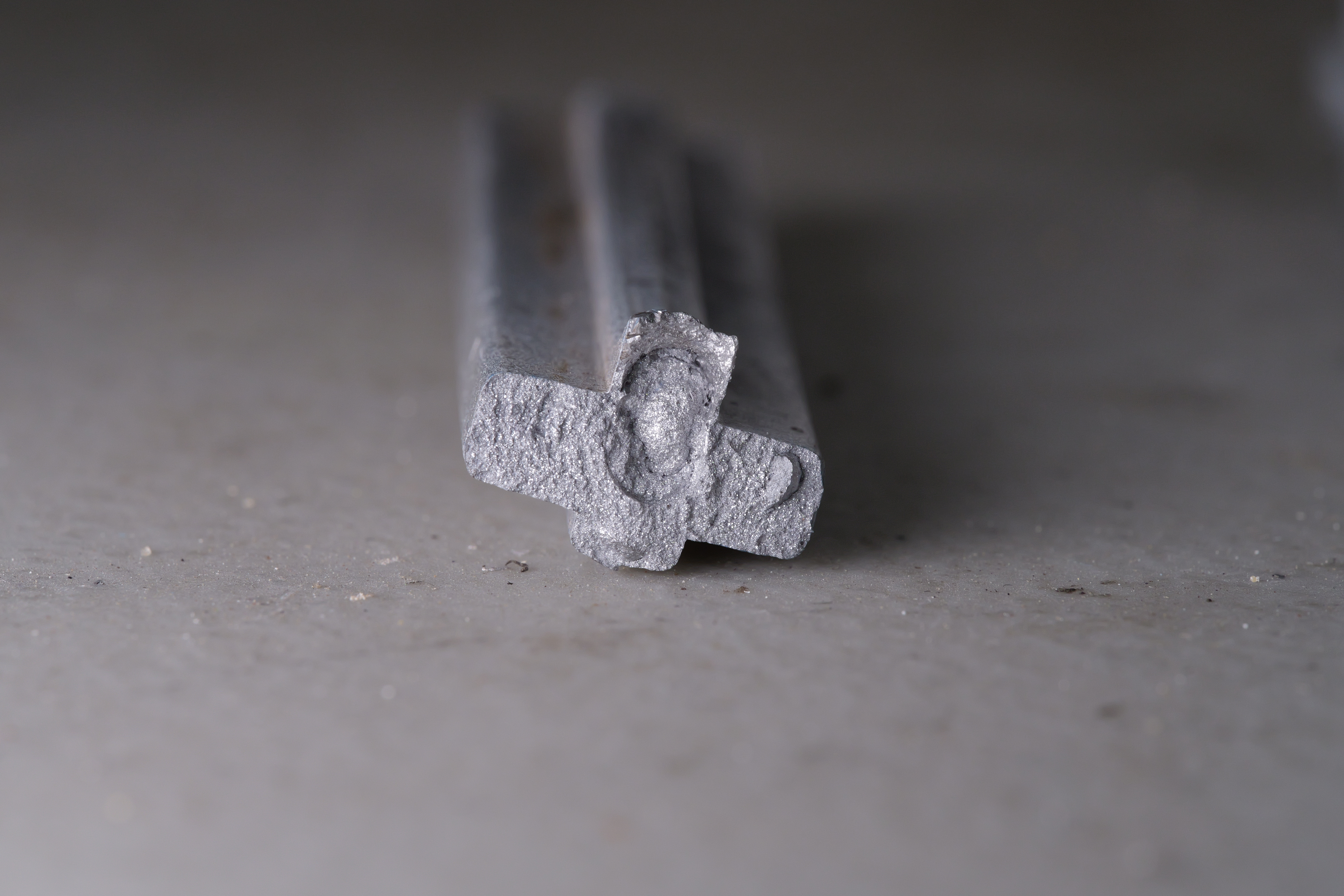
I really was not expecting the wheel to be the first mechanical part to break. But it was foreshadowed in this post, where I exposed the rim's casting voids while machining a new bearing pocket. I guess you get what you pay for with $20 cast aluminum rims. Here's where it might have failed first:
Interestingly, the new version of this rim has a different spoke geometry. I'll stop short of calling it better, though, without running some FEA and checking for voids. If it doesn't seem significantly improved, I might consider some other options for reinforcing them.
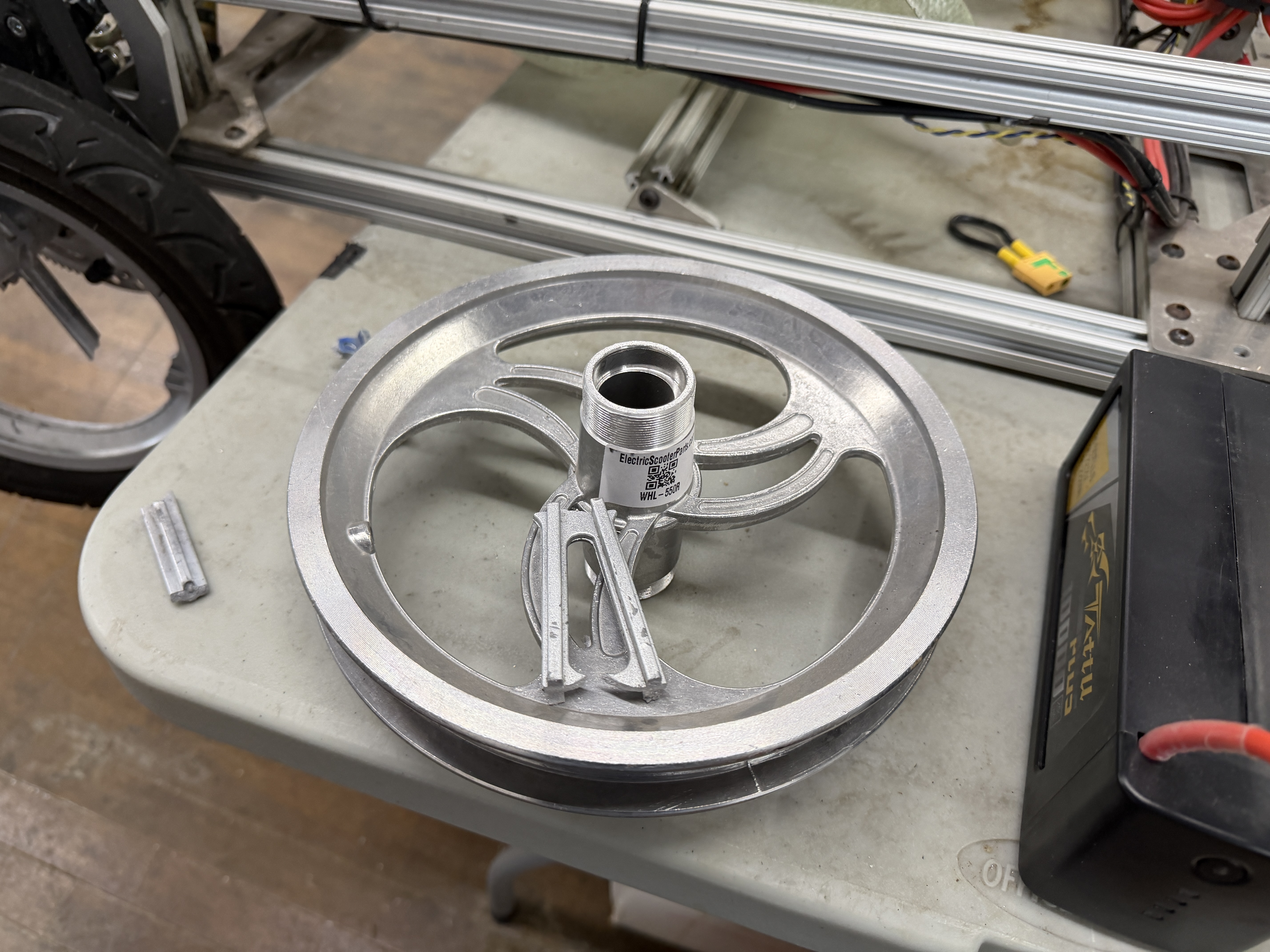
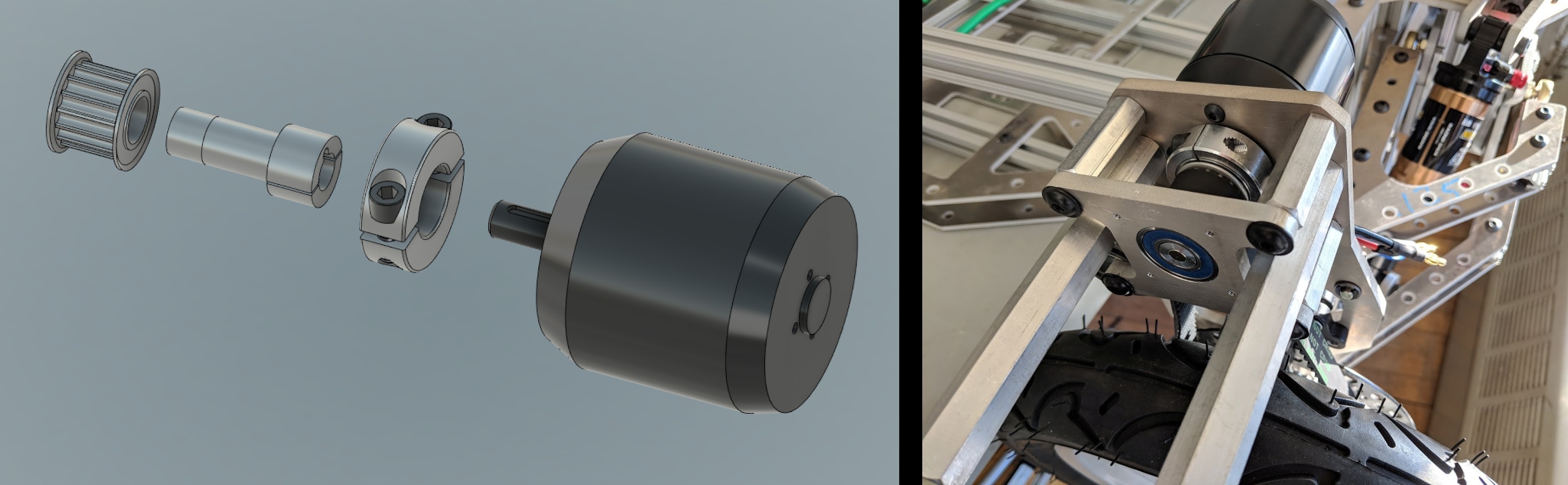
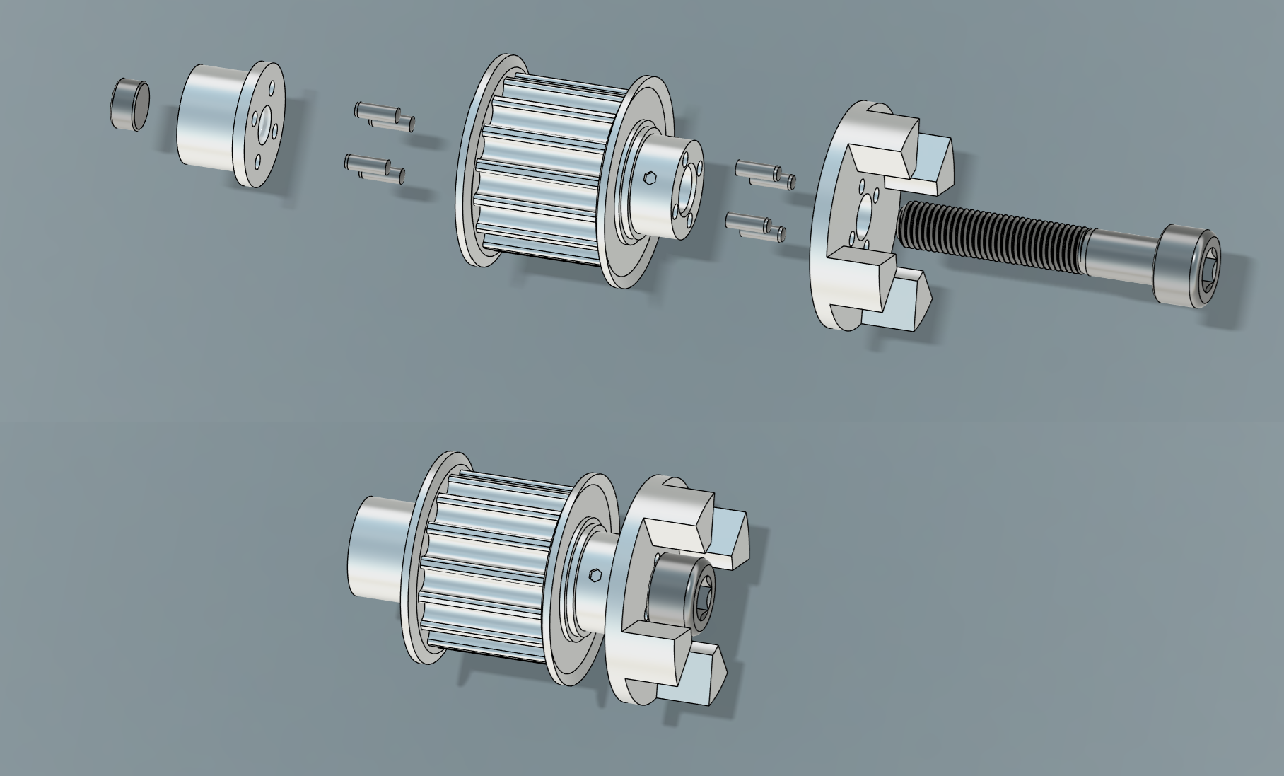
I'll probably just replace the two rear wheels, since they're the ones with the most weight and therefore the most side load on them. But I bought four new rims, just in case. I considered designing some billet-machined rims instead, but I think they'd cost a fortune and I'm not sure I'd be able to stop myself from trying to design in-wheel motors at that point.
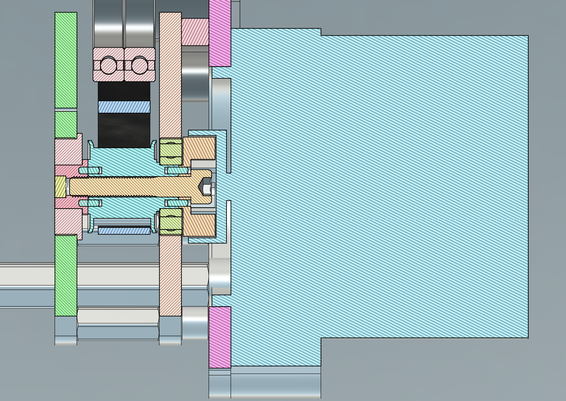
One other minor mechanical upgrade I've been wanting to make for a long time is to replace the steering u-joint. The current part is McMaster-Carr 6443K46, which has a tiny amount of play that I really dislike the feel of at the steering wheel. Maedler 63122200 is a much nicer part, and half the price! It will require a bit of redesign a re-machining of the steering column adapter, but I think it's worth it for a tighter steering feel.
I always plan to do all these upgrades during the summer and it never seems to happen. I wind up doing everything in the last few weeks leading up to ice racing. But maybe this year will be different!