
For hardware, I have my TE0803 carrier with the ZU4CG version of the TE0803. All I need for this test is JTAG, UART, and the four PL-side GT transceivers, for PCIe Gen3 x4. I made a JTAG + UART cable out of the Digilent combo part, which is directly supported in Vivado and saves a separate USB port for the terminal. Using Trenz's bare board files, it was pretty quick to set up.
 |
| TE0803 Carrier + Dead-Bugged Digilent JTAG+USB Adapter. |
Next, I wanted to validate the PCIe routing with a loopback test, following this video as a guide. I made my own loopback out of the cheapest M.2 to PCIe x4 adapter Amazon has to offer by desoldering the PCIe x4 connector and putting in twisted pairs. This worked out nicely since I could intentionally mismatch the length of one pair to get a negative result, confirming I wasn't in some internal loopback mode.
 |
| The three-eyed...something. |
For most of the rest of this test, I'm roughly following the script from the FPGA Drive example design readme files, with deviations for my custom board and for Vivado 2019.1 support. The scripts there generates a Vivado project and block design with the Processing System and the XDMA PCIe Bridge. I had a few hardware differences that had to be taken care of manually (EMIO UART, inverted SSD reset signal), but having a reference design to start from was great.
The example design includes a standalone application for simply checking that a PCIe drive enumerates on the bus, but it isn't built for the ZU+. As the readme mentions, there had been no standalone driver for the XDMA PCIe Bridge. Well, as of Vivado 2019.1, there is! In SDK, the standalone project for xdmapcie_rc_enumerate_example.c can be imported directly from the peripheral driver list in system.mss from the exported hardware.
Unfortunately, that's where the road seems to end in terms of quick and easy setup. The next stage involves PetaLinux, which is a toolchain for building the Xilinx Linux kernel. I don't know about other people, but every time the words "Linux" and "toolchain" cross my path, I automatically lose a week of time to setup and debugging. This was no exception.


 |
| XDMA standalone driver example is available as of Vivado 2019.1! |
I installed an SSD and ran this project and much to my amazement, the enumeration succeeded. By looking at the PHY Status/Control register at offset 0x144 from the Bridge Register Memory Map base address (0x400000000 here), I was also able to confirm that link training had finished and the link was Gen3 x4. (Documentation for this is in PG194.) Off to a good start, then.
 |
| Installed a 1TB Samsung 970 EVO Plus. |
Unsurprisingly, PetaLinux tools run in Linux. I went off on a bit of a tangent trying to see if they would run in WSL2. They do, if you contain your project in the Linux file system. In other words, I couldn't get it to work on /mnt/c/... but it worked fine if the project was in ~/home/... But, WSL2 is a bit bleeding edge still and there's no USB support as of now. So you can build, but not JTAG boot. If you boot from an SD card, though, it might work for you.
So I started over with a VirtualBox VM running Ubuntu 18.04, which was mercifully easy to set up. For reasons I cannot at all come to terms with, you need at least 100GB of VM disk space for the PetaLinux build environment, all to generate a boot image that measures in the 10s of MB. I understand that tools like this tend to clone in entire repositories of dependencies, but seriously?! It's larger than all of my other development tools combined. I don't need the entire history of every tool involved in the build...
 |
| And here I thought Xilinx was a disk space hog... |
The build process, even not including the initial creation of this giant environment, is also painfully slow. If you are running it on a VM, throw as many cores at it as you can and then still plan to go do something else for an hour. I started from the build script in the FPGA Drive example design, making sure it targetted cpu_type="zynqMP" and pcie_ip="xdma".
This should set up the kernel properly, but some of the config options in PetaLinux 2019.1 might not exactly match the packaged configs. There's a reference here explaining how to manually configure the kernel for PCIe and NVMe hosting on the Z-7030. I went through that, subbing in what I thought were correct ZU+ and XDMA equivalents where necessary. Specifically:
- It seems like as of PetaLinux 2019.1 (v4.19.0), there's an entire new menu item under Bus support for PCI Express Port Bus support. Including this expands the menu with other PCI Express-specific items, which I left at whatever their default state was.

- Under Bus support > PCI controller drivers, Xilinx XDMA PL PCIe host bridge support has to be included. I don't actually know if the NWL PCIe Core is also required, but left it in since it was enabled by default. It might be the driver for the PS-side PCIe?

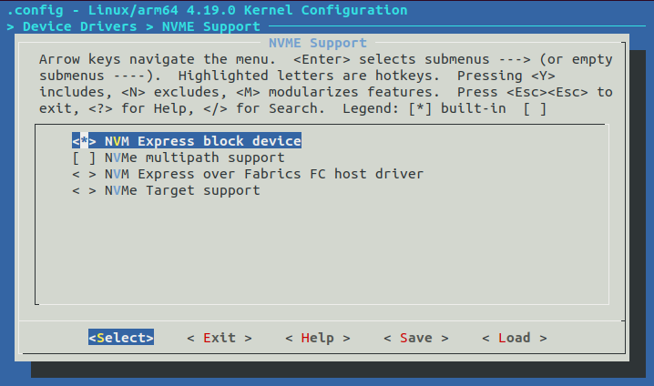
- Some things related to NVMe are in slightly different places. There's an item called Enable the block layer on the main config page that I assume should be included. Under Device Drivers, Block devices should be included. And under Device Drivers > NVME Support, NVM Express block device should also be included.
The rest of the kernel and rootfs config seems to match pretty closely the Z-7030 setup linked above. But I will admit it took me three attempts to create a build that worked, and I don't know exactly what trial-and-error steps I did between each one. Even once the correct controller driver (pcie-xdma-pl.c) was being included in the build, I couldn't get it to compile successfully without this patch. I don't know what the deal is with that, but after that I finally got a build that would enumerate the SSD on the PCIe bus:
 |
| Output from lspci -vv confirms link speed and width. |
I had already partitioned the drive off-board, so I skipped over those steps and went straight to the speed tests as described here. I tested a few different block sizes and counts with pretty consistent results: about 460MB/s write and 630MB/s read.
 |
| Not sure about those correctable errors. I guess it's better than un-correctable errors. |
That is actually pretty fast, compared to the Z-7030 benchmark. The ZU+ and the new driver seem like they're able to make much better use of the SSD. But, it's still about a factor of two below what I want. There could be some extra performance to squeeze out from driver optimization, but at this point I feel like the effort will be better-spent looking into hardware acceleration, which has been demonstrated to get to 1GB/s write speeds, even on older hardware.
Since there's no published datasheet or pricing information for that or any other NVMe hardware accelerator, I'm not inclined to even consider it as an option. At very least, I plan to read through the open specification and see what actually is required of an NVMe host. If it's feasible, I'd definitely prefer an ultralight custom core to a black-box IP...but that's just me. In the mean time, I have some parallel development paths to work on.