
In the original Freight Train of Pixels post, I laid out three main technical challenges to building a continuous recording 3.8Gpx/s imager. All three have now been dealt with, using a Zynq Ultrascale+ SoC as a hardware base. The detailed implementations for each one has its own post:
[The Pipe] - Hardware wavelet compression engine.
[The Sink] - Sustained 1GB/s writing to an NVMe SSD.
Now it's time to put all three pieces together and run it as a full pipeline:
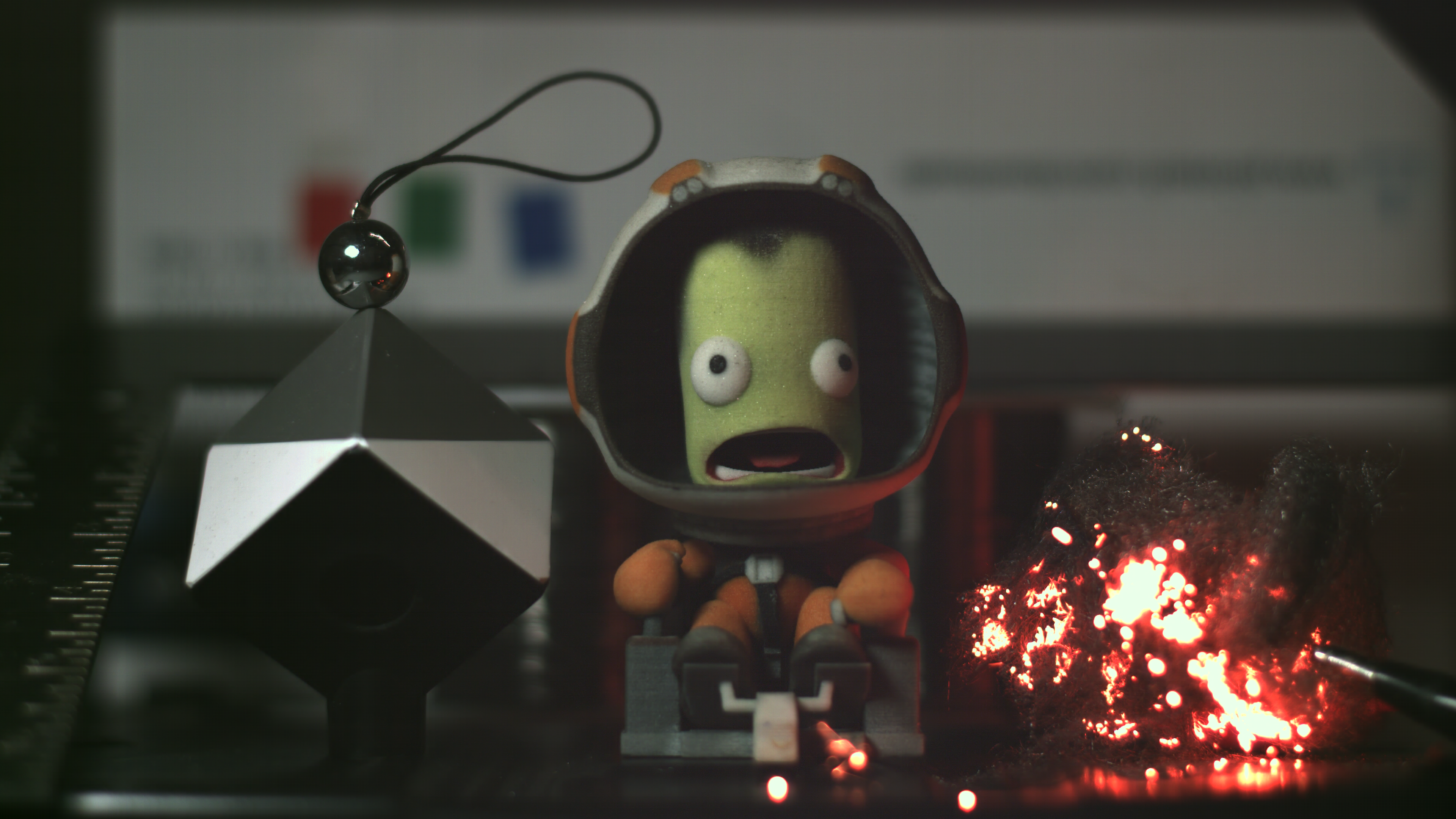
Since YouTube uploads are at the mercy of H.264, here's a PNG frame as well.
There are lots of technical details to dive into, but the first thing to point out is that this is 12000 frames of continuously-recorded 4K 400fps video. That's 30s in real-time and 500s of playback at 24fps, something very few existing high-speed imaging systems can do. And I can keep going. This clip is "only" 24GB of a 1TB SSD. To fill the entire 1TB would take about 20 minutes at this bit rate. That's 20 minutes of real-time, 5.5 hours of playback at 24fps.
This is made possible mostly due to the insane speed of modern SSDs. High-speed cameras typically use RAM to buffer raw frame data in real-time, transferring short clips to non-volatile storage after the capture period. But with NVMe flash write speeds now well into the GB/s range, maybe continuous direct recording to a single drive (or a RAID 0 array) will catch on. Besides the ability to capture long clips, it also allows an alternative trigger-free user interface that would be familiar to anyone: push to record, push to stop.
 |
| The real MVP here is the 1TB Samsung 970 Evo Plus NVMe SSD, a good example of modern consumer electronics running laps around everything above it in the pro/industrial world. |
I also picked a good hardware platform for this project: the lower-end Zynq Ultrascale+ SoCs, like that of the wonderful XCZU4CG module I've been using, have just barely enough resources to pull it off. I'm using 134 of the 144 LVDS-capable I/O, all four PCIe Gen3-capable transceivers, and most of the programmable logic. I was actually going to move up to the XCZU6, which has more than double the logic, but it seems to be on a different branch of the product tree that a) doesn't have PCIe hard blocks and b) isn't supported by Vivado HL WebPACK. For now, I'll just try my best to optimize for the XCZU4. I still have the XCZU5 and XCZU7 available to me if needed, though.
 |
| XCZU4 module transferred over to the v0.2 carrier, which has some new connectors including a barrel jack for power in, a full-size HDMI out, and some isolated GPIO. |
Most importantly, I felt confident enough in the design now to risk a color sensor on this board. Unlike my stockpile of monochrome CMV12000s from eBay, I bought this one new, at full price, and I do not want to break it. I haven't had any power supply issues in months of testing on the v0.1 board, so after a thorough multimeter check on the v0.2 board, I permanently soldered on the color sensor and crossed my fingers.
 |
| My one and only CMV12000-2E5C1PA, now committed to this board. |
Returning to the integration of the three main pieces of the image capture pipeline, there were a handful of small but important details to sort out regarding how frames are buffered in RAM and how they are written out to files on the SSD:

- The AXI Master port on the Encoder module now transfers data from the 16 compressor codestream FIFOs to RAM in increments of 512B, one logical block / sector on disk. This greatly simplifies downstream file writing operations.
- The (now sector-aligned) addresses of the next RAM write for each compressor codestream are presented to software via the Encoder module's AXI Slave. These addresses increment automatically as data is written, but can be overwritten by software.
- The CMV Input module generates an interrupt at the start of the Frame Overhead Time (FOT), a short (~20-30μs) period of deadtime between frame readouts where there shouldn't be any RAM writing happening.
- During the FOT interrupt, software reads the Encoder RAM write addresses, resets them if necessary, and records the start address and size of each compressor codestream for a given frame as part of a 512B frame header. Frame headers are stored in a circular buffer in RAM.
- In the main loop, frames are dequeued from RAM as needed by writing the frame header, followed by each of the 16 codestreams it references, to a file with FatFs. A new file is created every so often to prevent the file size from exceeding the 4GiB FAT32 limit.
This is all pretty easy to implement, at least compared to the three main hardware modules themselves. Most of it is ARM software, which can be iterated and debugged much faster than programmable logic. Also, having the codestream RAM address and size baked into the frame header helps with validating and analyzing the output:


The codestream size per frame shows how bandwidth is being distributed to the 16 codestreams, with more bits per frame going to the low-frequency subbands. Compression ratios relative to raw 10-bit data are shown on the codestream size axis. Spikes can be seen during the portions of the clip where the steel wool burns brightest. There's also a gradual increase in codestream size over the 30 seconds, especially in the high-frequency subbands, which I believe is due to image sensor noise increasing with temperature. Feeding the codestream size back into the quantizer settings to maintain a roughly constant bit rate will be a problem for another day.
 Each codestream is given a range of RAM addresses to use as a circular buffer for frame data. At the start of a clip, the encoder RAM write addresses are set to the bottom of their range. As data is written, the addresses increment automatically. When they reach the top of their range, software resets them during the FOT interrupt. Each codestream does this independently, but the overall frame buffering capability is limited by the most frequently reset stream. In this case, XX3 resets approximately every 400 frames, so a maximum of 1s can be buffered. Ideally, the RAM ranges would be sized proportionally to the codestream bit rates to maximize the number of frames that can be buffered.

The RAM frame buffer allows the pipeline to ride out NVMe writing delays that last for several frame intervals. Each frame is time stamped once when it is read into RAM and again when it is submitted for writing to the SSD. The two time stamps and the frame write backlog count are added to the frame header, and can be used to review the delay.


Here, the read-to-read interval between frames is a steady 2.5ms, as it must be for 400fps. (A spike would indicate a dropped frame.) The read-to-write delay is typically 10ms, corresponding to a four frame backlog. This offset is set by software to allow for a small number of frames between the read and write pointer, which could be used to generate a low-latency local preview. There is a spike in read-to-write delay every 240 frames when a new file is created, since the file creation NVMe operations are slower than streaming writes. Most of these spikes are only one frame, but there were instances of higher delays, up to 20 total frames (50ms). This is still easily absorbed by the RAM buffer, although it would be good to understand where the extra delay comes from.
So all 12000 frames (113.2Gpx) made it onto the SSD in 30 seconds. That's the last stop on the freight train of pixels - once they hit the flash, they're no longer volatile or time-critical. So in some sense this project is done. But from a practical standpoint, there's still an equal amount of computation that has to happen to decode the frames and run the inverse DWTs, not to mention the additional load of debayering, color correction, and eventual transcoding. What the ZU+ does at 400fps, my laptop CPU struggles to undo at 0.25fps. So implementing decode and inverse DWT in a GPU-accelerated way just became high-priority. Luckily, I remember that I do at least have an existing GPU debayer and color correction solution.
I had to do a little work to modernize it, but since laptop hardware has also gotten way better since I wrote it, it can scrub through 4K raw just fine. Hopefully, I can implement the decode and IDWT there as well, to save the 4s per frame it currently takes to do those on the CPU. I'll also need the ZU+ to be able to do it, for preview and playback, but since it only has to run at 30fps that should be much easier than the forward direction.
Besides that, there are a few side-challenges I still have to take on:
- The HDMI output, so I can see what the hell I'm doing. This will involve some amount of decoding and inverse DWT, at least of the 3rd and maybe 2nd wavelet stage, to generate a usable preview image with a menu and status overlay. I don't have the ability to output 4K, so a 1080p preview will have to suffice.
- USB mass-storage device access to the SSD. As much as I love my Sabrent NVMe SSD enclosure, I fear I am approaching the insertion/removal cycle limit on this drive. I have already demonstrated USB 3.0-speed mass storage device access to ZU+ RAM, so this should be a simple SCSI bridge project. Bonus points if I can implement a few custom SCSI commands to start/stop recording or do other useful control tasks.
- An alternative programmable logic configuration for the CMV12000's subsampled read-out mode. In this mode, the X and Y read-out skips every other 2x2 Bayer block, for a maximum resolution of 2048x1536 at a frame rate of 1050fps. Or an even more interesting 1472fps at 1080p. Because this mode reads in four rows in parallel, it will require more Stage 1 Horizontal DWT Cores, which might be tough on the XCZU4.
But having the full capture pipeline in place is a good milestone, and I'm happy that it's pretty close to what I had in mind back in June. Some of the details changed as I learned about the capabilities and limitations of the ZU+, but the high-level architecture is as-planned. Being able to capture 3.8Gpx/s continuously (for less than 5nJ/px, too) is something that I think is new and only recently possible with the latest generation SSDs and FPGA hardware working together. Keeping an eye on new components and trying to figure out interesting corner cases where they might be useful is something I enjoy, so this was a fun challenge.
Holy cow, how does one get to your level?
ReplyDeleteI've read all your posts about this project, what a ride. I almost bought from the same eBay listing as you, but in the end I decided not to, because I wasn't confident enough I could make a working design around it (plus import tax and duty made it less compelling, as I am not from the USA).
I have done some FPGA projects in the past, but none involving high-speed DDR connections so it has been a pleasure to observe your way of problem solving over the months.
You managed to achieve more in 6 months than the entire Apertus team did in 6 years, while providing worlds better documentation.
Do you have any intentions of open sourcing your project? I would be grateful if I could study your design to learn what it takes to achieve such a feat.
Thanks! To be fair, I have followed the Apertus project since they started and taken some architectural inspiration from them (CMV12000 + Zynq). The hardware I'm using didn't exist when they started, but their work with the MicroZed (Zynq 7020-based) that gave me confidence that the Zynq Ultrascale+ could do what I wanted. Maybe five years from now somebody else can make an 8K 1000fps version with a Zynq Megascale+++.
DeleteI will keep the HDL source for the key IP cores themselves here: https://github.com/coltonshane/WAVE-Vivado, under the MIT License. It's not enough to clone the whole project from scratch, but could be useful as a reference, together with the documentation here.
Wow.
ReplyDelete