Thursday, February 20, 2025

GaNDr: Power Loop Measurement and Optimization

In a half-bridge configuration, the power loop is the path from the DC bus capacitor positive terminal to the output switch node and back to the capacitor negative terminal. This is the path of high dI/dt, passing through both FETs in the half-bridge. It's important to keep this loop as small as possible, to reduce the amount of parasitic inductance interacting with the high dI/dt.

This applies to any half-bridge, but it's especially important for GaNFETs, where the switching event can be on the order of nanoseconds. They're capable of switching this fast due to their very low gate charge and input capacitance, but they still have a significant output capacitance, COSS, that needs to be hard-switched. During a switching event, this forms an underdamped LC oscillator with the power loop inductance and leads to overshoot and ringing.

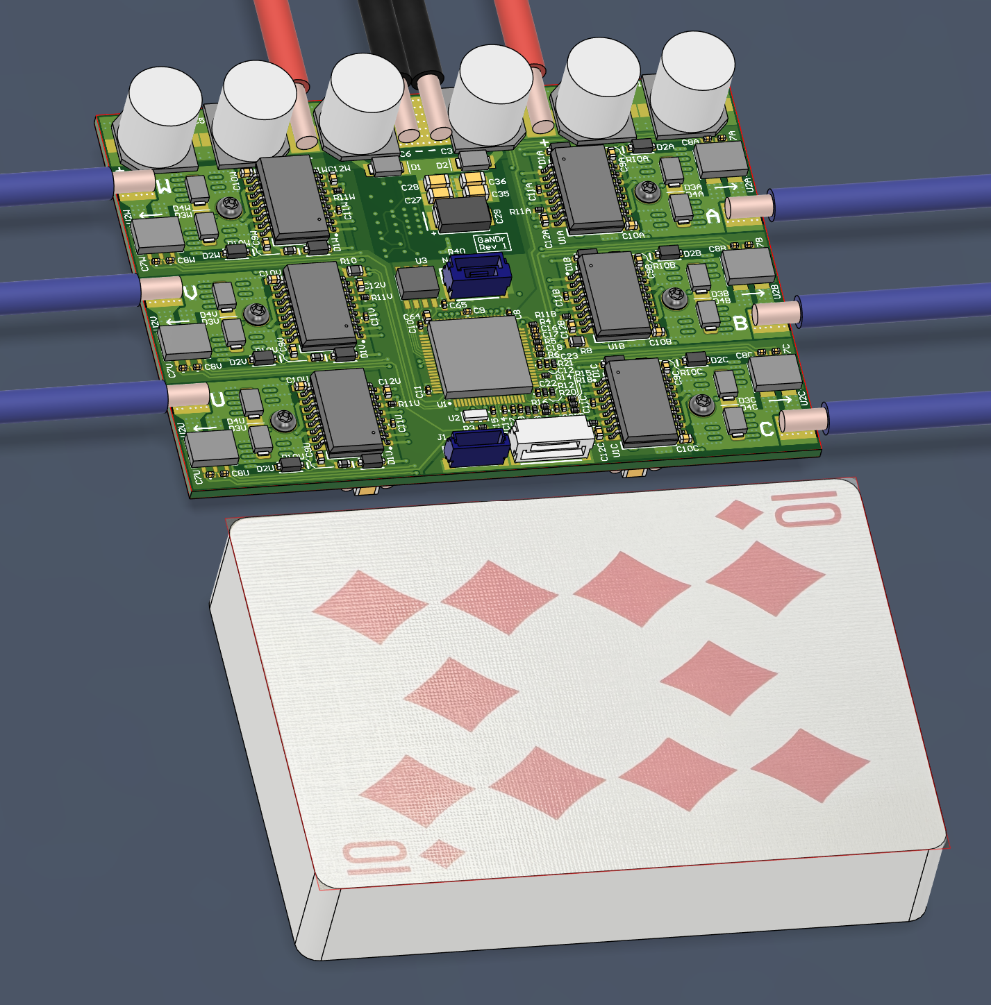
It's a little hard to predict the loop inductance, although admittedly I didn't even really try. There are ways to ballpark it based on the board geometry, or use a 2D field solver like FEMM to get an estimate. A 3D field solver could probably get pretty close. But nothing beats a direct measurement on the real PCB. So I just assembled one phase of the GaNDr Rev1 PCB for a test:

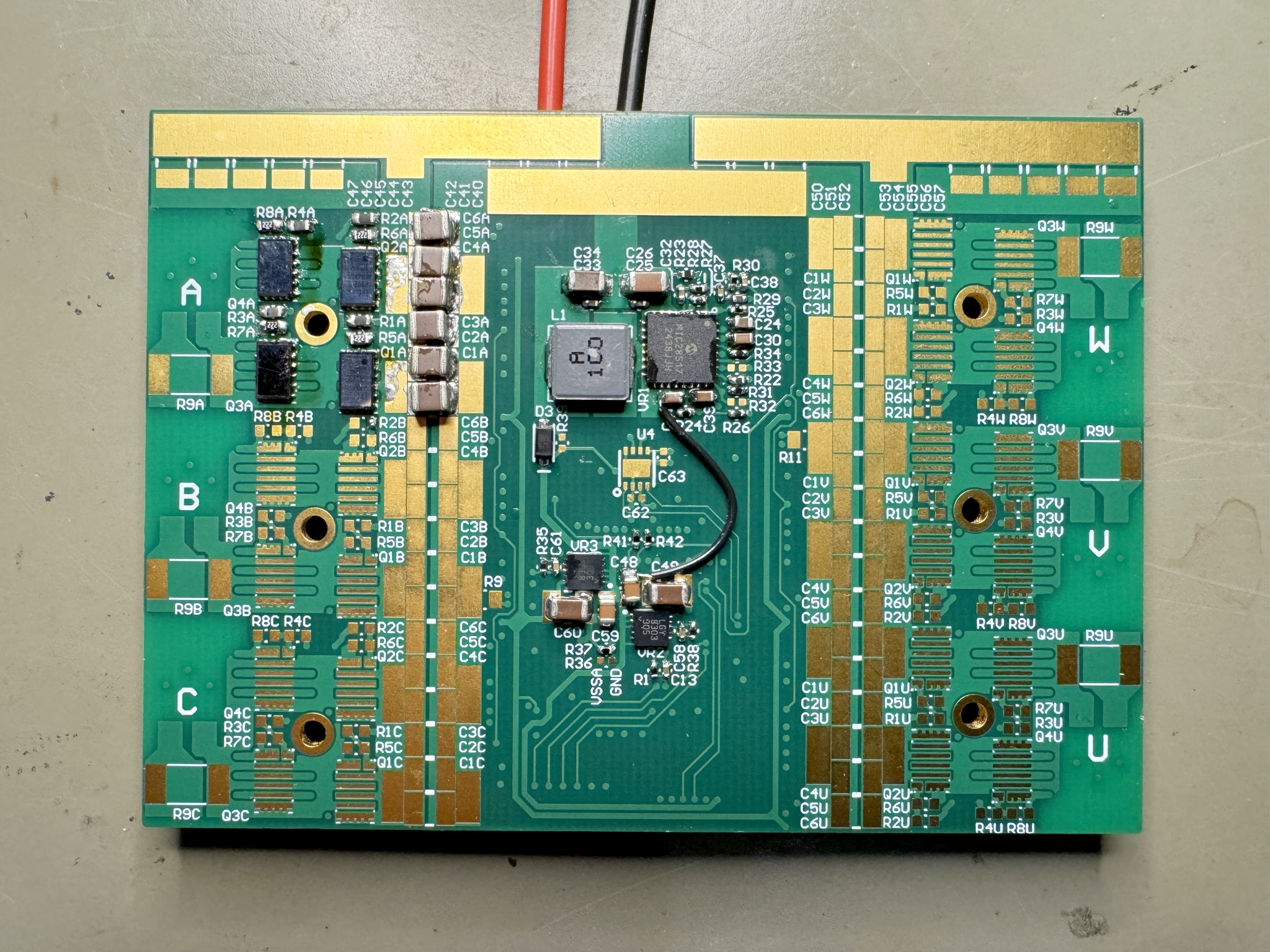
Nevermind the black wire hack...

Since I'm interested in stuff on the nanosecond time scale, I wanted to use my 5GHz-bandwidth sampling scope for this measurement. But the inputs only go up to ±1V, so directly probing a 50V node with unknown overshoot would be bad. Luckily, the cheapest way to make a high-bandwidth probe is just to make a voltage divider with a physically small resistor and a 50Ω coaxial cable.

Quick and dirty ≈67:1 high-bandwidth probe.

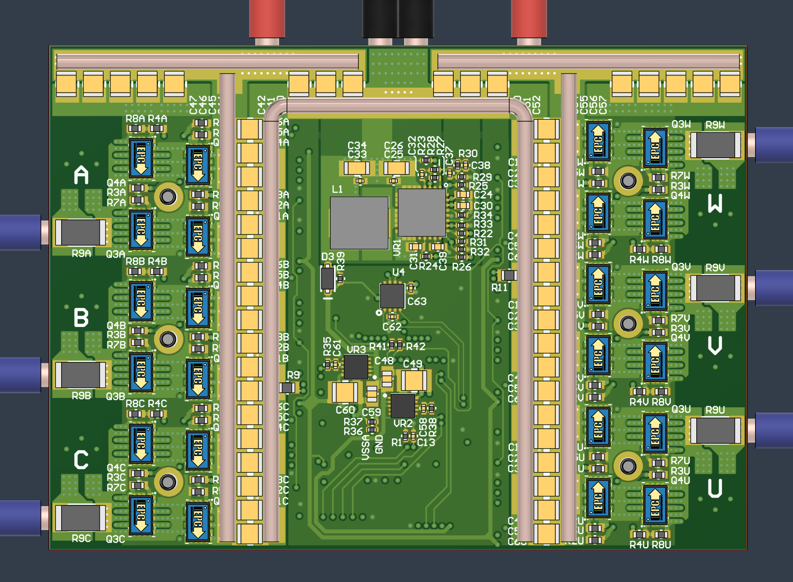
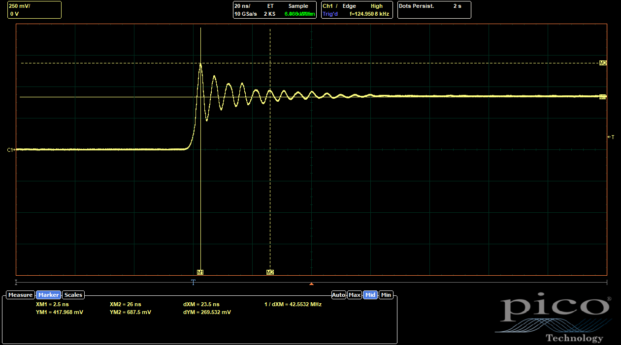
It also matters where the probe is attached. I soldered both the resistor and the probe ground (just the coax shield) to pads near the low-side FET. This excludes all the inductance except what's physically inside the FET. The measured voltage is, as close as possible, VDS of the low-side FET. And here is the measured switching transient:

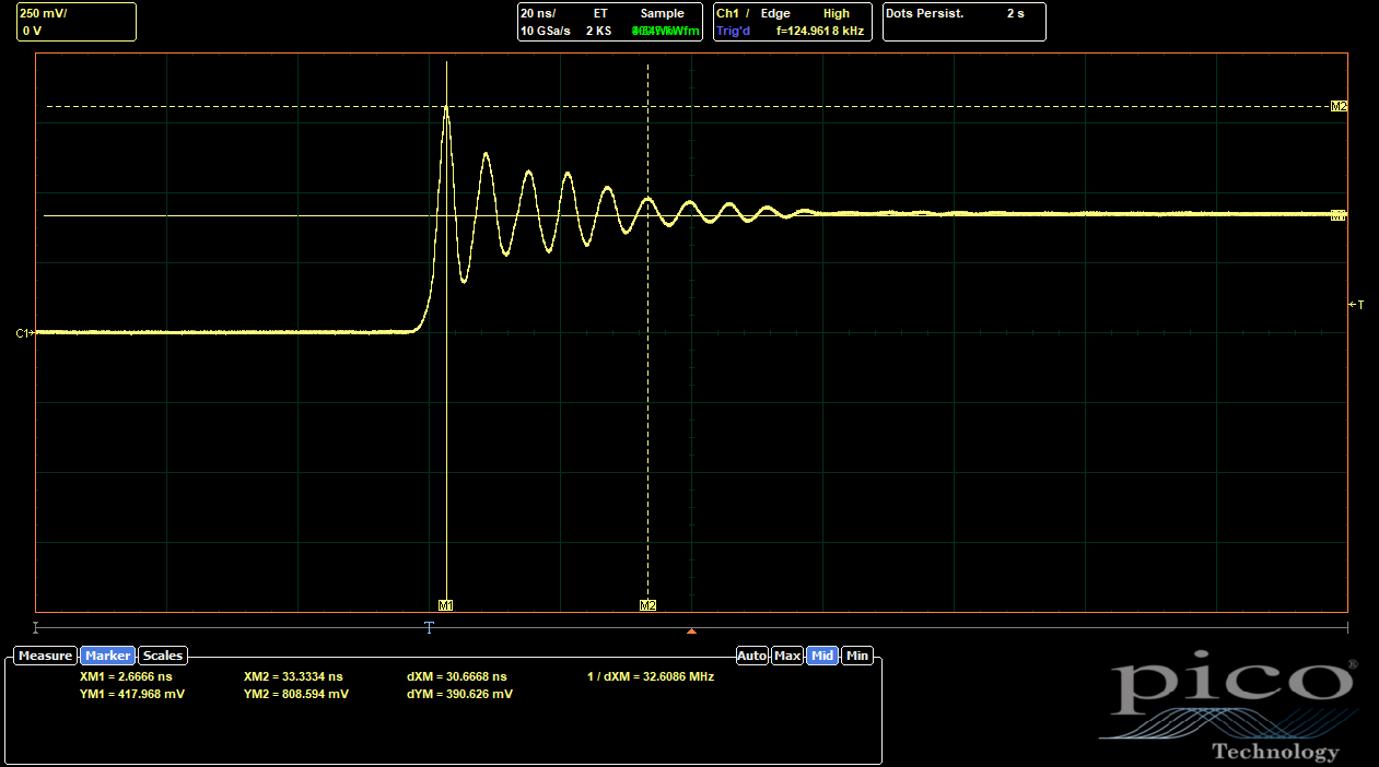
It is...not great. The overshoot with a 32V input and 1Ω gate resistors is nearly 100%. That does not bode well for 50V operation with 100V parts, and can't be good for efficiency or EMI. It's possible to slow down the rise time by increasing the gate resistance, thus reducing the amount of energy in the transient. But that should be done last, after exhausting all other reasonable methods for reducing the power loop inductance.

Since I now have the ringing frequency, it's possible to calculate the power loop inductance using the COSS datasheet value of 1nF (per FET):

L = 1 C OSS ( 2 π f ) 2 = 1 2.0 nF ( 2 π 160 MHz ) 2 = 0.50 nH

This really isn't much inductance, but it's apparently enough to store sufficient energy during the transient to make a high-Q oscillator with COSS.

Some of the loop inductance is from the DC bus capacitors themselves. I probably should have checked this earlier, since this is usually well-characterized by the manufacturer. The Samsung CL32E475KCIVPNE capacitors used here have the following AC characteristic curves:

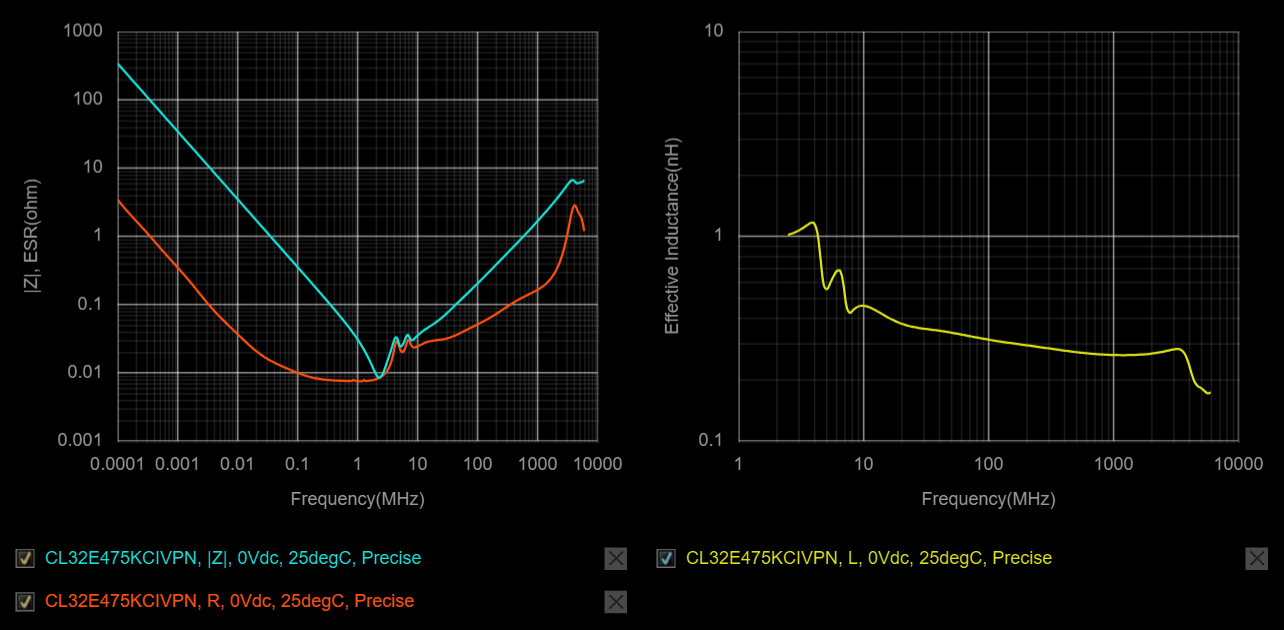
At frequencies above about 2MHz, they're really more inductors than they are capacitors: the impedance vs. frequency has a slope of +1 on a log-log plot. The effective inductance at 160MHz is around 0.30nH. But, there are six in parallel. Ideally, this would divide down to 0.050nH, but they may not share the load equally based on their placement. I think they contribute a significant amount of inductance, but not the majority.

Still, it would be nice to reduce the capacitor parasitic inductance if possible. Since the switching transient only involves COSS, which is only on the order of 1nF, maybe smaller and faster capacitors would be better? For example, the 10nF Samsung CL05B103KC5VPNC in 0402 stays mostly capacitive all the way up to 100MHz:

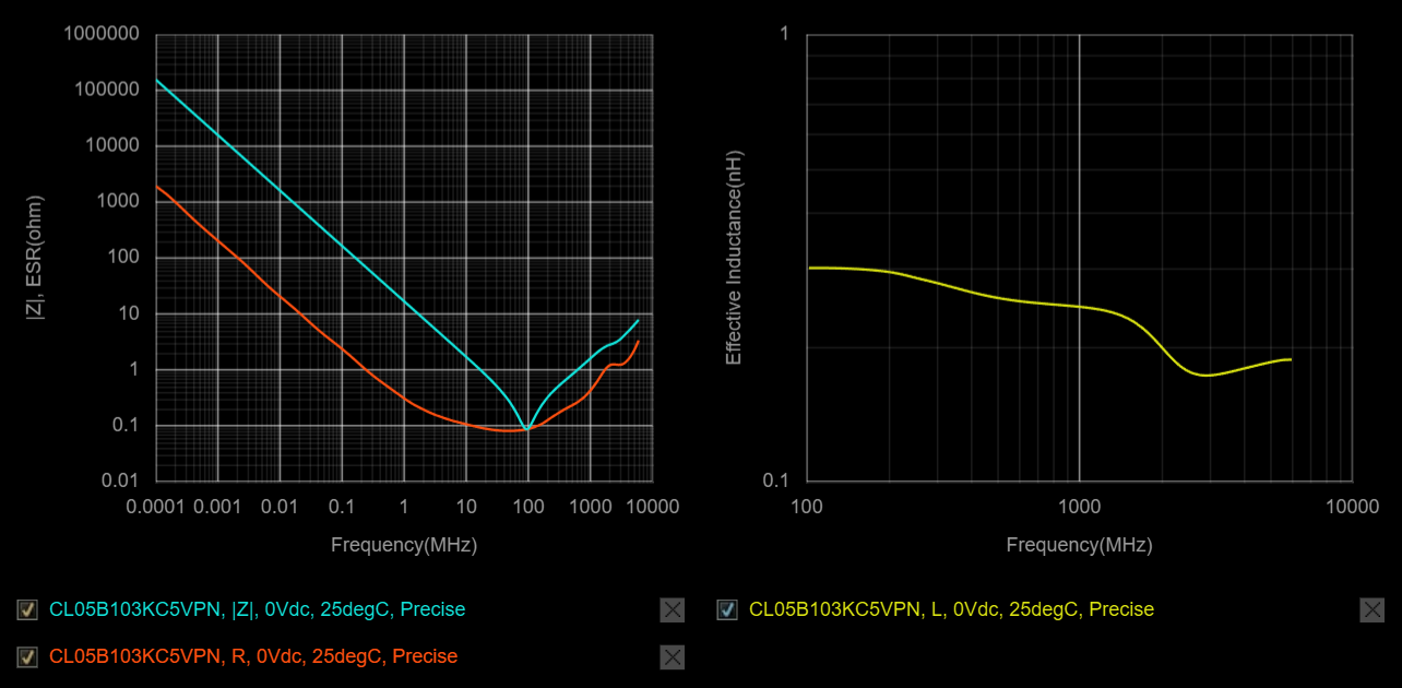
However, being physically smaller also increases the impedance overall, such that the effective inductance at 160MHz is still around 0.30nH. The advantage is that I could fit many more in parallel, to divide down the total inductance more. In reality, the big 1210 capacitors are still very much necessary for filtering the 125kHz PWM frequency, so the solution is probably to try to fit some of the 10nF 0402s on in parallel with the existing six 1210s.

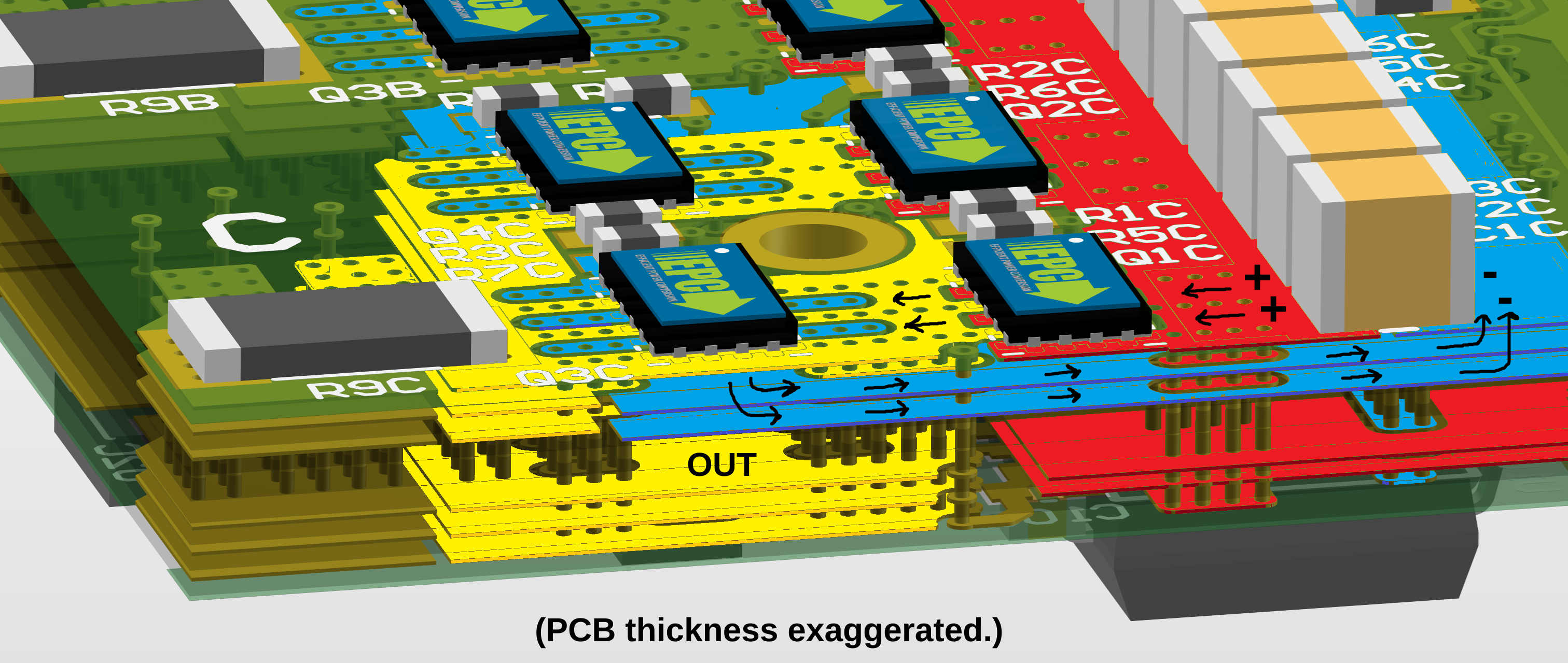
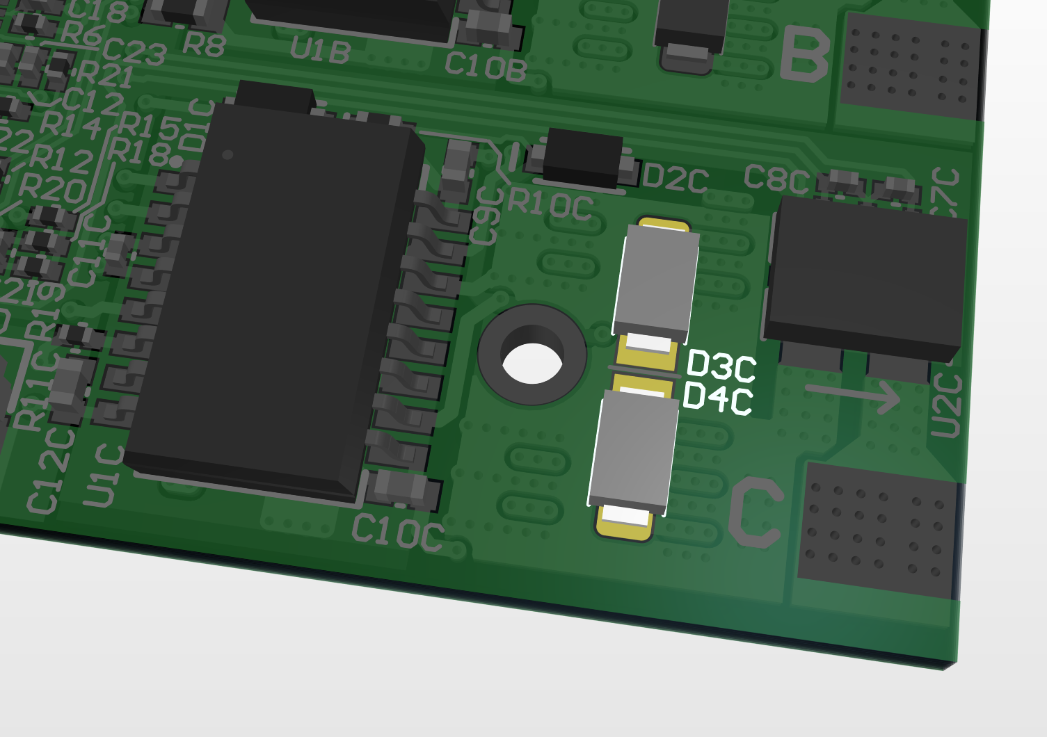
An easy place to put them is where the VDC bus bar solder areas used to be, between the 1210 caps and the high-side FETs:

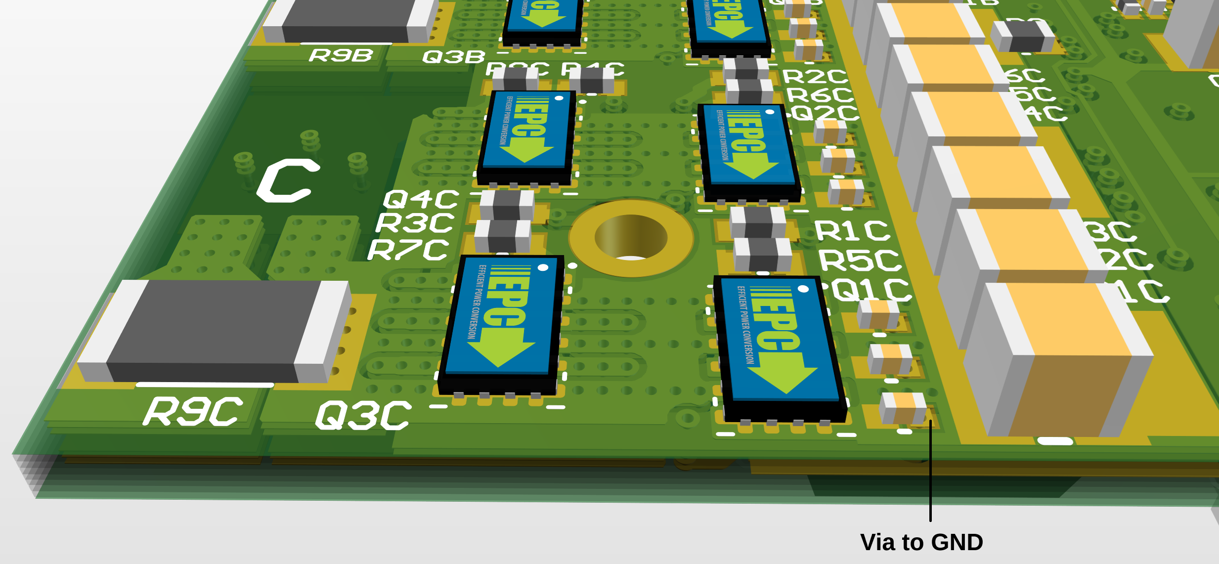
For each high-side FET, three can be arranged so that their positive terminals are directly adjacent to the drain pads. The negative terminal can be sent to the power ground plane on the first inner layer with a via-in-pad. This also has the advantage of shortening the power loop considerably, at least for the high-frequency switching transient. The only real disadvantage is losing the option for a VDC bus bar, which realistically shouldn't be necessary for the average power levels here.

A riskier move would be to drop in four more 10nF 0402s between the FETs:

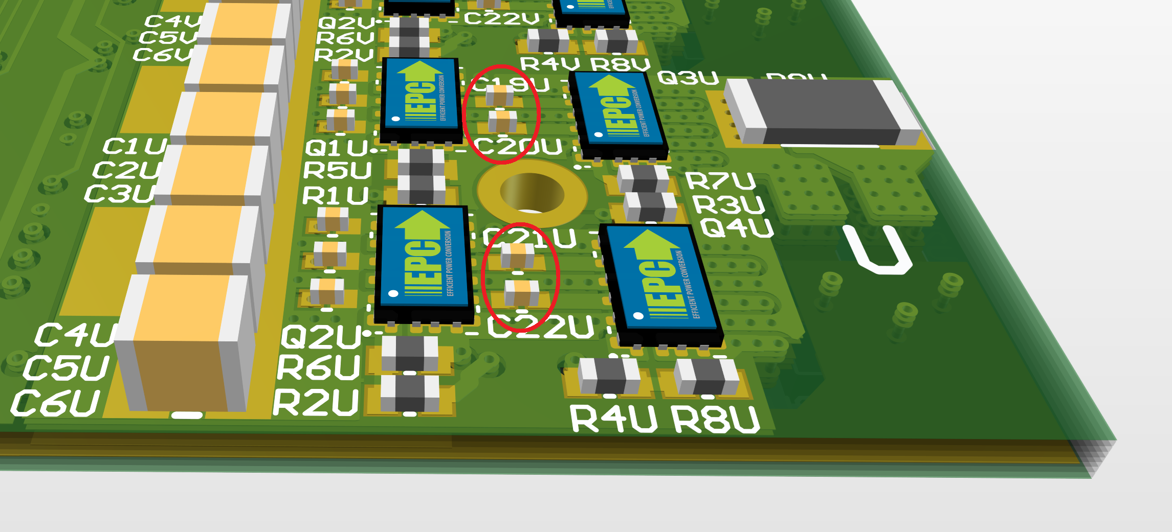
The drain pads of the high-side FET (VDC) align with the source pads of the low-side FET (GND), so it's very tempting to bridge the gap with an 0402 capacitor. I even tried this on the physical board, by scratching off some solder mask:

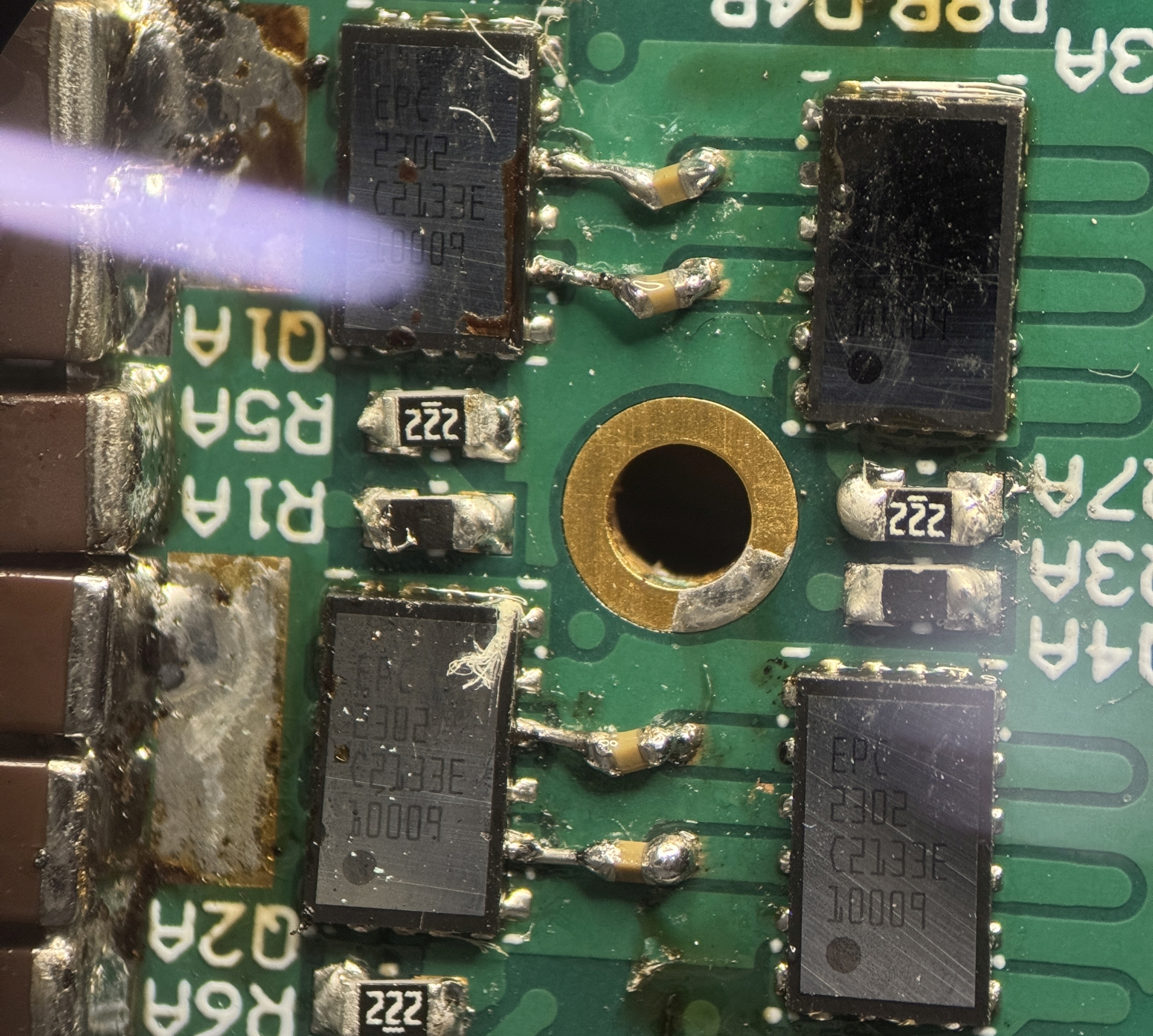
Even with the ugly attachment, this did show a significant improvement, with the overshoot dropping from 94% to 65% and the frequency increasing from 160MHz to 210MHz:

This does seem like it would provide the shortest possible power loop, but an important difference between the soldered-on test and the actual layout is that there is still a mostly solid switch node (output) plane beneath the capacitors as-tested. It's like having a seventh PCB layer. In actuality, that plane gets cut if the capacitors are placed there, changing the power loop from a thin vertical sandwich to multiple horizontal loops, which might very well have higher inductance.

This configuration, with capacitors between the FETs, is actually discussed in the EPC layout guidelines. In order to get back to a thin vertical sandwich power loop, the switch node plane, rather than GND, should be on the first inner layer. But if I fully swap SW and GND layers, the loop sandwich to the outer capacitors becomes thicker, potentially cutting off those capacitors with much higher outer loop inductance.

I decided to try just inserting a small SW plane on the first inner layer, and only between the FETs. The rest of the first and second inner layers remains as GND to hopefully preserve some of the outer capacitor loop performance. And since I'm indecisive, I only did this on one half of the board for the next revision. That'll let me A/B test it against the more normal layout. I expect both to have much more interesting transients with composites of multiple frequencies, so it might be trickier to analyze. We'll see when the Rev 2 boards arrive.

Saturday, January 25, 2025

GaNDr: Motor Drive in the GaNFET Era

It's been a while since I've attempted a new motor drive design, the last one being TinyCross's dual-motor 50V/100A drive about six years ago. I still really like that design, and those drives have worked well for TinyCross so far. But one of my favorite pastimes is looking for new components that might change how I would build something. And in the last six years, there's been an interesting development that I'm curious to explore: the GaNFET is now mainstream. 

While they've been commercially available for a while, they're now both technically and economically viable as an alternative to silicon MOSFETs in certain power ranges, and have been adopted in many new consumer electronic devices. They are also becoming available in more conventional packages, though GaNFET purists would probably still use the bare-die versions for lowest parasitic inductance. Supporting components (mainly gate drivers), documentation, and device models are also now mature and widely available.

Of interest for this project are the EPC2302 and the brand new EPC2361 in 3x5 QFN. These are packaged GaNFETs, vs. the bare-die BGA and LGA options that have been around for a while. Ideally, encapsulating them in a thin plastic package improves robustness without sacrificing too much performance. The package also still exposes the die on the top side for direct cooling.

GaNFETs excel in the Figure-of-Merit (FoM) of on-resistance multiplied by gate charge, RDS(on)·QG, which captures both the conducting and switching losses. Here they are on a 2D plot with some silicon MOSFETs for comparison, with curves of constant FoM shown (lower is better):

The current TinyCross FETs, FDMT80080DC, can't really compete anymore. (I still love them for their pulsed current rating of 1453A, though.) The modern field of 60-80V silicon MOSFETs has significantly better FoM and also tends to publish specifications for lower gate drive voltages besides the standard 10V. The NVMFS5C604NL operated at VGS = 4.5V is especially remarkable. But the EPC GaNFETs still easily win on FoM, and they are 100V parts with half the surface area.

The extremely low QG means GaNFETs can be switched much faster than silicon MOSFETs. An EPC2302 half-bridge with a suitable layout and gate driver should have no problem operating at 100kHz PWM, or even higher. This reduces the need for large electrolytic capacitors on the DC bus, since the ripple current will be much lower. This is probably the largest contribution to space savings, even though the FETs themselves are also physically smaller.

Although I'm not space-constrained on TinyCross, shrinking a power stage is always a fun project. I arbitrarily set a limit of the size of a deck of cards, with the same specification as the previous design (dual motor, 50V and 100A peak). Here's what the resulting layout looks like:

It's considerably smaller than the current TinyCross drive, even with the logic and power consolidated onto one board. There are half as many electrolytic capacitors, with more ceramic capacitors filling in at high frequencies. Optional 2mm bus bars help take some of the load off the PCB copper. The board can be mounted to a heat sink base with six isolated M2 screws located in the middle of each FET group for even mounting pressure. And the wires all exit horizontally, probably through grommets in the seam between the aluminum base and a 3D-printed cover.

This is also a six-layer PCB, which further helps with layout. Six layer boards are now pretty fast and cheap thanks with JLCPCB, so there's not much reason to stick to four layers even for hobby motor drives anymore. The power stage layout follows EPC's recommended structure pretty closely, with the return path on the two inner layers closest to the FETs to minimize the dI/dt loop area:

I did not follow the gate drive recommendations as strictly, since I need a lot of space for the gate drivers themselves. I am using isolated half-bridge drivers, and remarkably there are at least two pin-compatible parts from different manufacturers that could work. The Skyworks Si82E39x looks like the most promising option, with a 4V UVLO option and sub-10ns rise/fall times. It's not even that expensive, at around $4ea. The ADuM4221 from Analog Devices could also work, though. Although I have the driver on the opposite side of the board, I did try to keep the gate drive traces as short as possible:

The gate drive return paths from the switch node (high-side) and negative plane (low-side) are also pretty direct. Will that be good enough? I don't really know - I don't have a 3D field solver. I'll have to wait for the boards. Ideally, with such low gate charge and fast drivers, it should be possible to run PWM frequencies above 100kHz and take the dead time down to around 50ns (less than 1%). Here's what the switching waveforms look like in an LTSpice simulation with the EPC device models:

However, this is just a guess for the loop inductance, so I won't really know how fast it can go until I get it on a scope. But what is the huge current spike on both FETs (shoot-through) during the high-side turn-on? I thought GaNFETs didn't have reverse recovery time? Well, I think it's just the Coss of the low-side FETs getting charged. Even though there's no body diode, there is still parasitic capacitance in the 1-2nF (per FET) range that has to get hard-switched at 50V. At these switching speeds, that requires a lot of current (for a very short period of time). If it turns out to be a problem, the gate drives will have to be artificially slowed down with extra gate resistance.

Another interesting quirk of GaNFETs is present in the LTSpice sim: during the deadtime, the low-side FETs do reverse-conduct, but at a voltage of around 2.25V, significantly higher than the body diode voltage across a silicon MOSFET. This partially eats into the power savings of a GaNFET design, but the more critical problem is what happens with a bootstrapped high-side driver. If the output is down at -2.25V, or even lower, even a crappy bootstrap diode won't drop enough from +5V to prevent the high-side VGS from exceeding 6V, the absolute maximum for these gates.

There are several ways to deal with this. Adding a resistor in series with the bootstrap diode creates low-pass filter with the bootstrap capacitor. A 10Ω resistor with a 0.1µF bootstrap capacitor has a time constant of 1µs, so a 50ns spike of +7V or so won't budge the voltage much. There is still a possibility that at very high duty cycle the average bootstrap charge voltage could exceed 6V, but I think you would run into other issues before that. For good measure, I also included a footprint for an optional 5.1V Zener diode across the bootstrap cap, which is another recommendation I saw.

Lastly, I included a couple footprints for small Schottky diodes in parallel with the low-side FETs. I can only fit something like an SMA or SOD128 package, which max out at 5A for 100V devices. But some have pulse ratings at or above 100A, and these are very short pulses. At those pulse ratings the voltage drop is quite high, but still significantly below 2.25V. The other interesting question is whether the parasitic inductance of the diode and its connection to the bridge will prevent any of the high current from making it to them in the first place. Only the scope will tell.

In order to take advantage of the 100kHz+ low-deadtime PWM, I also want to try out another relatively new part, an MCU from the STM32G4 series. These are the spiritual successor to the F3 series that I've used for so many motor drives. They have lots of analog features, including five (!) ADC converters, DACs, op-amps, and comparators. But the G4 also adds several new peripherals that are specifically well-suited to motor drives:

The high-resolution timer (HRTIM) can drive up to 12 PWM outputs with a resolution as small as 184ps. It's probably overkill, but it allows for close to 16-bit duty cycle resolution at 100kHz, and very accurate deadtime control. For example, part-to-part variation in the gate driver propagation delays could probably be compensated There's also a CORDIC engine for offloading trigonometric functions from the CPU. And there's a Filter Math Accelerator (FMAC) peripheral, which includes a dedicated hardware multiplier/accumulator and memory for accelerating FIR/IIR filter calculations without involving the CPU.

The need for extra computation might make more sense if you've noticed what's missing from this design: there are no inputs for motor position sensing. While I love the simplicity and robustness of TinyCross's optically-isolated virtual Hall sensors, it's nothing interesting in terms of brushless motor control. I did manage to run two instances of a lightweight flux observer in the background on the F3, but I never used it for driving the current control. I'm sure it would have worked at speed, but the main problem with sensorless control for TinyCross is getting starting torque on all four drive motors without them fighting each other.

One way to get the position of the motor before the flux observer converges is with High-Frequency Injection (HFI). The motors on TinyCross have an L/R time constant of around 1.5ms, so at frequencies above 1kHz they are mostly inductors. The inductance on each phase varies depending on the position of the rotor, since the permanent magnet flux changes where each phase's stator steel is on a non-linear B-H curve. That inductance change can be measured with a high-frequency signal on top of the normal drive voltage to derive the position. This is nothing new - it's been basically perfected in VESC - but it should be fun to try to implement with 100kHz+ PWM and the STM32G4's extra processing power.

That's it for now - more to come when there is physical hardware to look at.