In a half-bridge configuration, the power loop is the path from the DC bus capacitor positive terminal to the output switch node and back to the capacitor negative terminal. This is the path of high dI/dt, passing through both FETs in the half-bridge. It's important to keep this loop as small as possible, to reduce the amount of parasitic inductance interacting with the high dI/dt.
This applies to any half-bridge, but it's especially important for GaNFETs, where the switching event can be on the order of nanoseconds. They're capable of switching this fast due to their very low gate charge and input capacitance, but they still have a significant output capacitance, COSS, that needs to be hard-switched. During a switching event, this forms an underdamped LC oscillator with the power loop inductance and leads to overshoot and ringing.
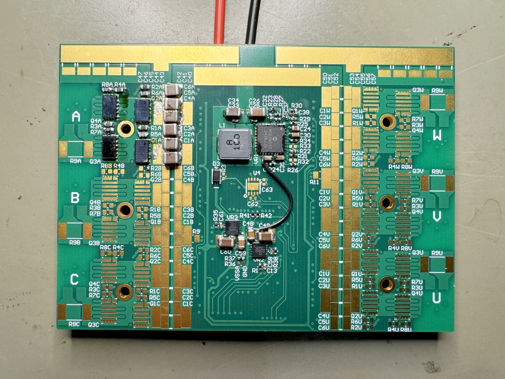
It's a little hard to predict the loop inductance, although admittedly I didn't even really try. There are ways to ballpark it based on the board geometry, or use a 2D field solver like FEMM to get an estimate. A 3D field solver could probably get pretty close. But nothing beats a direct measurement on the real PCB. So I just assembled one phase of the GaNDr Rev1 PCB for a test:
 |
| Nevermind the black wire hack... |
Since I'm interested in stuff on the nanosecond time scale, I wanted to use my 5GHz-bandwidth sampling scope for this measurement. But the inputs only go up to ±1V, so directly probing a 50V node with unknown overshoot would be bad. Luckily, the cheapest way to make a high-bandwidth probe is just to make a voltage divider with a physically small resistor and a 50Ω coaxial cable.
 |
| Quick and dirty ≈67:1 high-bandwidth probe. |
It also matters where the probe is attached. I soldered both the resistor and the probe ground (just the coax shield) to pads near the low-side FET. This excludes all the inductance except what's physically inside the FET. The measured voltage is, as close as possible, VDS of the low-side FET. And here is the measured switching transient:
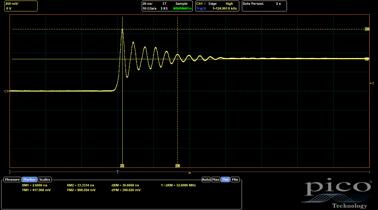
It is...not great. The overshoot with a 32V input and 1Ω gate resistors is nearly 100%. That does not bode well for 50V operation with 100V parts, and can't be good for efficiency or EMI. It's possible to slow down the rise time by increasing the gate resistance, thus reducing the amount of energy in the transient. But that should be done last, after exhausting all other reasonable methods for reducing the power loop inductance.
Since I now have the ringing frequency, it's possible to calculate the power loop inductance using the COSS datasheet value of 1nF (per FET):
This really isn't much inductance, but it's apparently enough to store sufficient energy during the transient to make a high-Q oscillator with COSS.
Some of the loop inductance is from the DC bus capacitors themselves. I probably should have checked this earlier, since this is usually well-characterized by the manufacturer. The Samsung CL32E475KCIVPNE capacitors used here have the following AC characteristic curves:
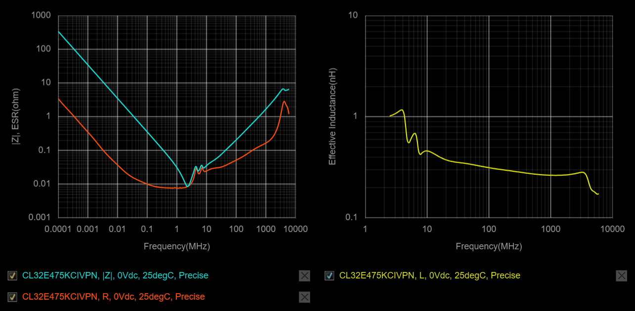
At frequencies above about 2MHz, they're really more inductors than they are capacitors: the impedance vs. frequency has a slope of +1 on a log-log plot. The effective inductance at 160MHz is around 0.30nH. But, there are six in parallel. Ideally, this would divide down to 0.050nH, but they may not share the load equally based on their placement. I think they contribute a significant amount of inductance, but not the majority.
Still, it would be nice to reduce the capacitor parasitic inductance if possible. Since the switching transient only involves COSS, which is only on the order of 1nF, maybe smaller and faster capacitors would be better? For example, the 10nF Samsung CL05B103KC5VPNC in 0402 stays mostly capacitive all the way up to 100MHz:
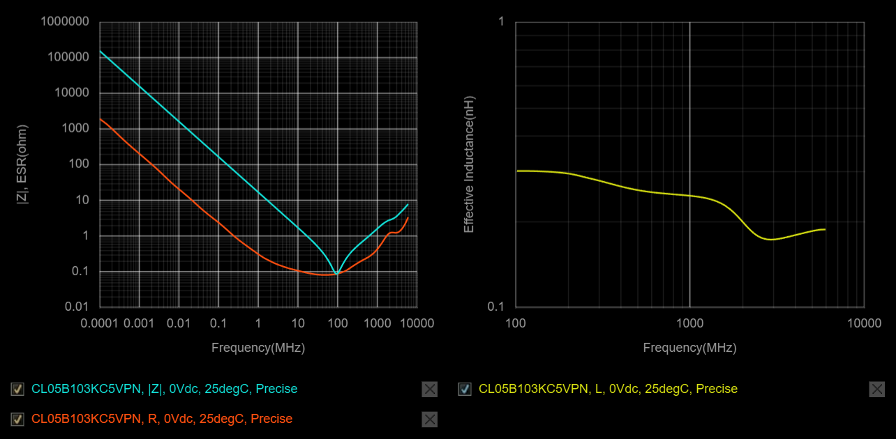
However, being physically smaller also increases the impedance overall, such that the effective inductance at 160MHz is still around 0.30nH. The advantage is that I could fit many more in parallel, to divide down the total inductance more. In reality, the big 1210 capacitors are still very much necessary for filtering the 125kHz PWM frequency, so the solution is probably to try to fit some of the 10nF 0402s on in parallel with the existing six 1210s.
An easy place to put them is where the VDC bus bar solder areas used to be, between the 1210 caps and the high-side FETs:
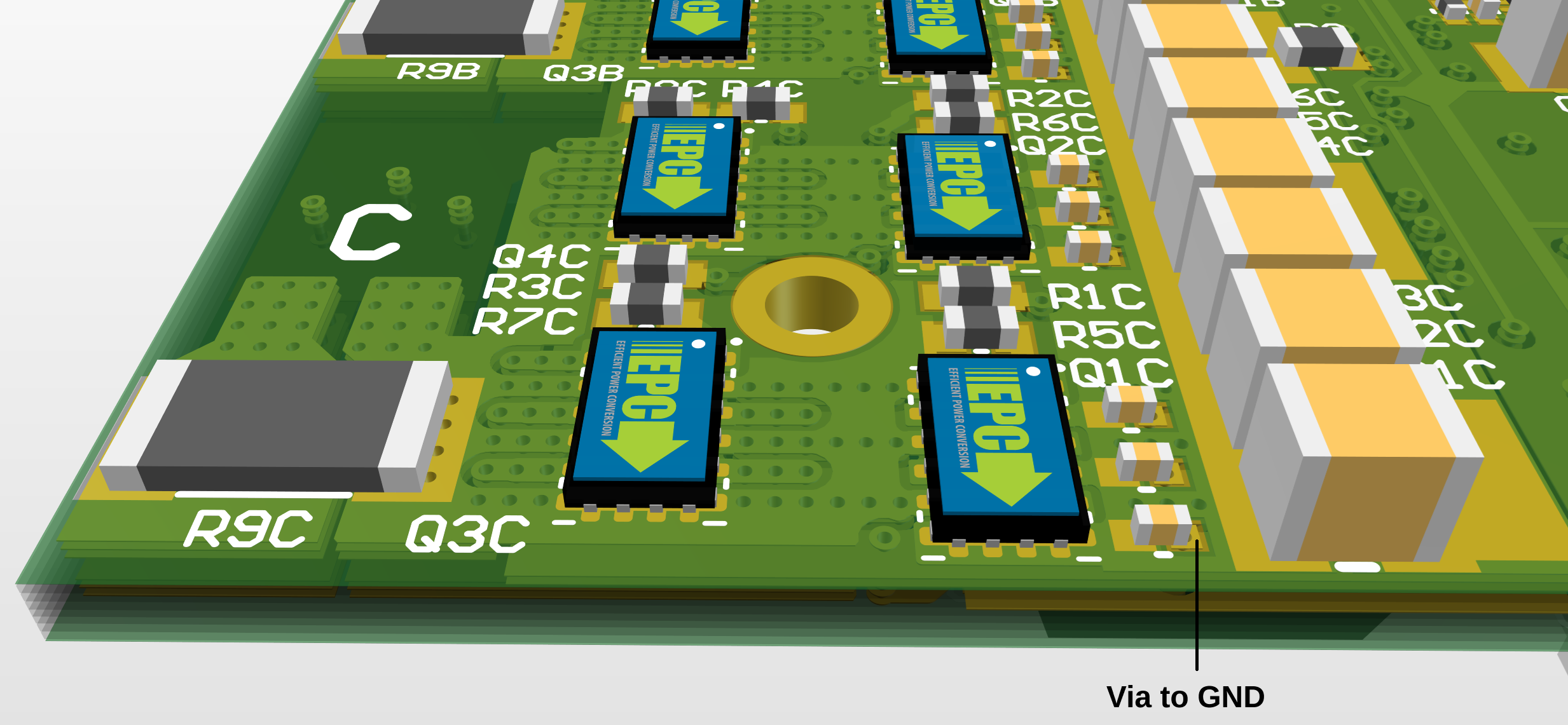
For each high-side FET, three can be arranged so that their positive terminals are directly adjacent to the drain pads. The negative terminal can be sent to the power ground plane on the first inner layer with a via-in-pad. This also has the advantage of shortening the power loop considerably, at least for the high-frequency switching transient. The only real disadvantage is losing the option for a VDC bus bar, which realistically shouldn't be necessary for the average power levels here.
A riskier move would be to drop in four more 10nF 0402s between the FETs:
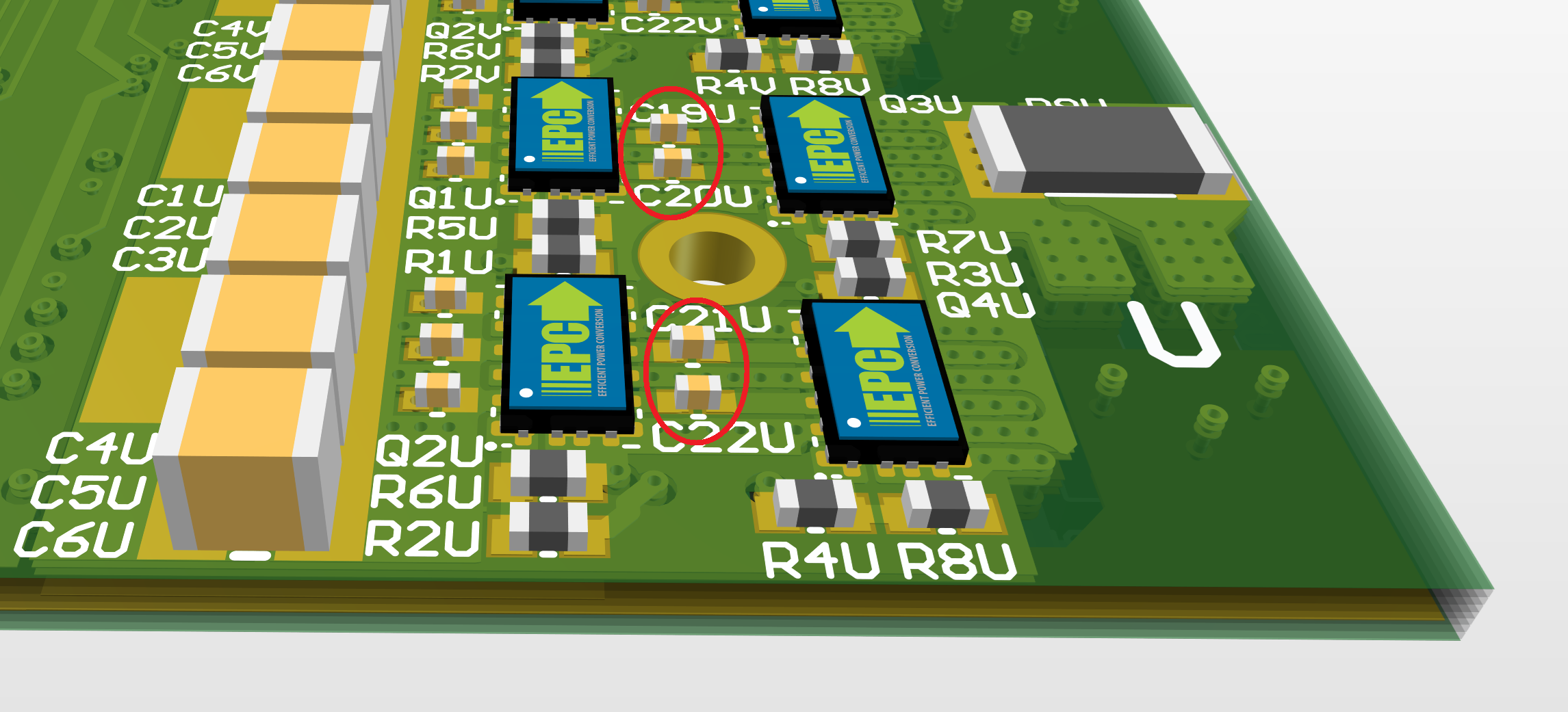
The drain pads of the high-side FET (VDC) align with the source pads of the low-side FET (GND), so it's very tempting to bridge the gap with an 0402 capacitor. I even tried this on the physical board, by scratching off some solder mask:
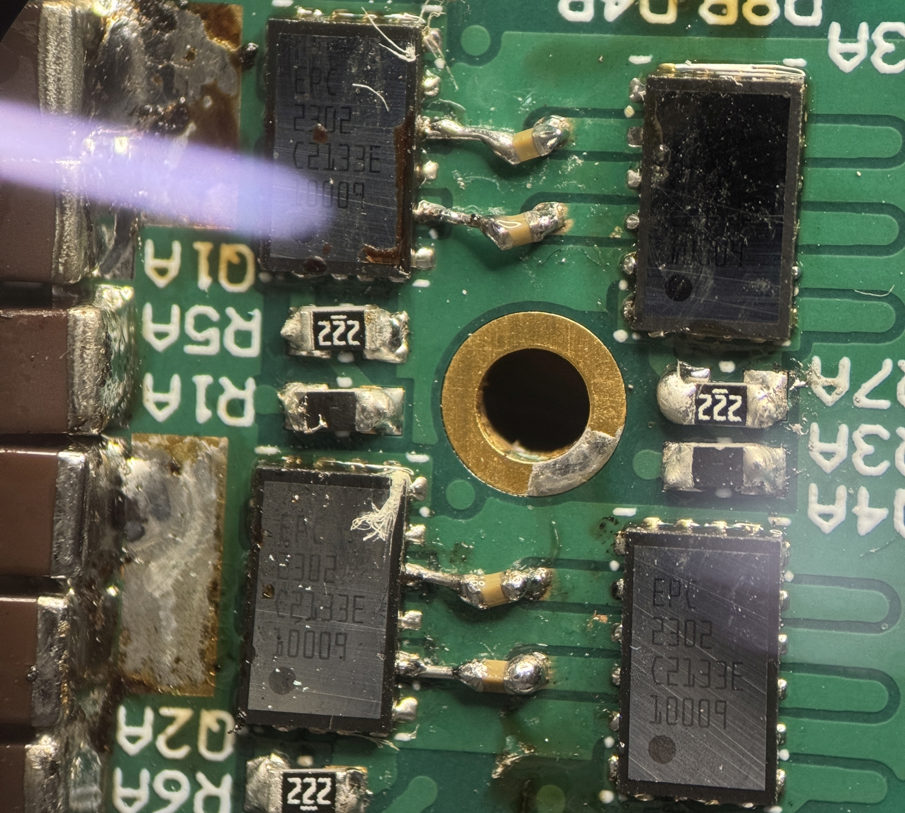
Even with the ugly attachment, this did show a significant improvement, with the overshoot dropping from 94% to 65% and the frequency increasing from 160MHz to 210MHz:
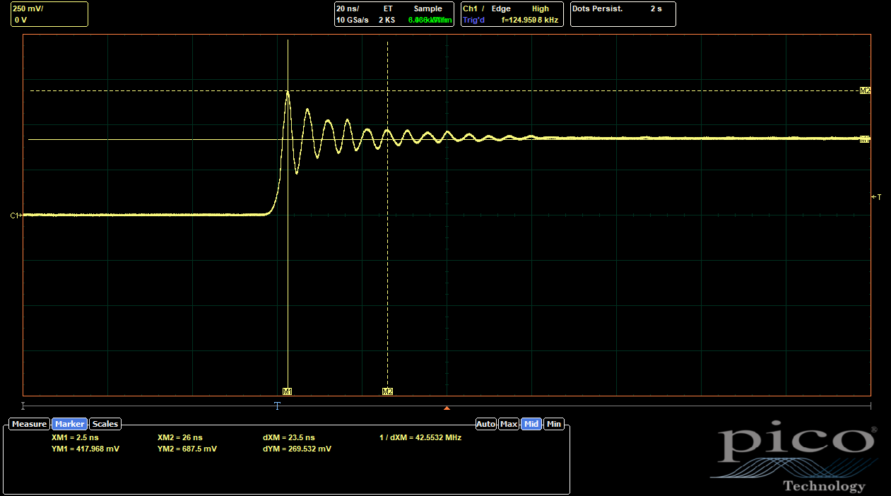
This does seem like it would provide the shortest possible power loop, but an important difference between the soldered-on test and the actual layout is that there is still a mostly solid switch node (output) plane beneath the capacitors as-tested. It's like having a seventh PCB layer. In actuality, that plane gets cut if the capacitors are placed there, changing the power loop from a thin vertical sandwich to multiple horizontal loops, which might very well have higher inductance.
This configuration, with capacitors between the FETs, is actually discussed in the EPC layout guidelines. In order to get back to a thin vertical sandwich power loop, the switch node plane, rather than GND, should be on the first inner layer. But if I fully swap SW and GND layers, the loop sandwich to the outer capacitors becomes thicker, potentially cutting off those capacitors with much higher outer loop inductance.
I decided to try just inserting a small SW plane on the first inner layer, and only between the FETs. The rest of the first and second inner layers remains as GND to hopefully preserve some of the outer capacitor loop performance. And since I'm indecisive, I only did this on one half of the board for the next revision. That'll let me A/B test it against the more normal layout. I expect both to have much more interesting transients with composites of multiple frequencies, so it might be trickier to analyze. We'll see when the Rev 2 boards arrive.

