In the original Freight Train of Pixels post, I laid out three main technical challenges to building a continuous recording 3.8Gpx/s imager. All three have now been dealt with, using a Zynq Ultrascale+ SoC as a hardware base. The detailed implementations for each one has its own post:
[The Source] - Full-speed read-in of the CMV12000's 64 LVDS channels.
[The Sink] - Sustained 1GB/s writing to an NVMe SSD.
Now it's time to put all three pieces together and run it as a full pipeline:
Since YouTube uploads are at the mercy of H.264, here's a PNG frame as well.
There are lots of technical details to dive into, but the first thing to point out is that this is 12000 frames of continuously-recorded 4K 400fps video. That's 30s in real-time and 500s of playback at 24fps, something very few existing high-speed imaging systems can do. And I can keep going. This clip is "only" 24GB of a 1TB SSD. To fill the entire 1TB would take about 20 minutes at this bit rate. That's 20 minutes of real-time, 5.5 hours of playback at 24fps.
This is made possible mostly due to the insane speed of modern SSDs. High-speed cameras typically use RAM to buffer raw frame data in real-time, transferring short clips to non-volatile storage after the capture period. But with NVMe flash write speeds now well into the GB/s range, maybe continuous direct recording to a single drive (or a RAID 0 array) will catch on. Besides the ability to capture long clips, it also allows an alternative trigger-free user interface that would be familiar to anyone: push to record, push to stop.
The real MVP here is the 1TB Samsung 970 Evo Plus NVMe SSD, a good example of modern consumer electronics running laps around everything above it in the pro/industrial world.
Of course, the other enabling factor is the use of wavelet compression to reduce the data rate by a ratio of at least 5:1. This might seem like cheating, but since a similar compression ratio is utilized by REDCODE, Blackmagic RAW, Apple ProRes RAW, and probably many other "raw" formats, I don't feel the least bit guilty. On a sensor like the CMV12000, a lightweight compression pass might actually help the image quality, since it'll inherently denoise the image somewhat.
I also picked a good hardware platform for this project: the lower-end Zynq Ultrascale+ SoCs, like that of the wonderful XCZU4CG module I've been using, have just barely enough resources to pull it off. I'm using 134 of the 144 LVDS-capable I/O, all four PCIe Gen3-capable transceivers, and most of the programmable logic. I was actually going to move up to the XCZU6, which has more than double the logic, but it seems to be on a different branch of the product tree that a) doesn't have PCIe hard blocks and b) isn't supported by Vivado HL WebPACK. For now, I'll just try my best to optimize for the XCZU4. I still have the XCZU5 and XCZU7 available to me if needed, though.
XCZU4 module transferred over to the v0.2 carrier, which has some new connectors including a barrel jack for power in, a full-size HDMI out, and some isolated GPIO.
Although I'm sticking with the same ZU+ module, I did finally get around to building a new carrier. The main addition is an HDMI transmitter, which I'll probably play with in the coming weeks. There's also a new barrel jack power input and an isolated GPIO connector. Other than a PCIe reference clock routing fix, I didn't touch any of the existing high-speed signals. I also (re)discovered good drag soldering technique, so there were zero issues with the 160-pin headers this time around.
Most importantly, I felt confident enough in the design now to risk a color sensor on this board. Unlike my stockpile of monochrome CMV12000s from eBay, I bought this one new, at full price, and I do not want to break it. I haven't had any power supply issues in months of testing on the v0.1 board, so after a thorough multimeter check on the v0.2 board, I permanently soldered on the color sensor and crossed my fingers.
My one and only CMV12000-2E5C1PA, now committed to this board.
The wavelet compression engine was designed for the Bayer-masked color sensor, with independent encoding for each color field, so I didn't have to change any hardware or software to accommodate it. All the color processing happens off-board, a point of reckoning discussed below. But from an image capture point of view, it's 100% drop-in.
Returning to the integration of the three main pieces of the image capture pipeline, there were a handful of small but important details to sort out regarding how frames are buffered in RAM and how they are written out to files on the SSD:
The AXI Master port on the Encoder module now transfers data from the 16 compressor codestream FIFOs to RAM in increments of 512B, one logical block / sector on disk. This greatly simplifies downstream file writing operations.
The (now sector-aligned) addresses of the next RAM write for each compressor codestream are presented to software via the Encoder module's AXI Slave. These addresses increment automatically as data is written, but can be overwritten by software.
The CMV Input module generates an interrupt at the start of the Frame Overhead Time (FOT), a short (~20-30μs) period of deadtime between frame readouts where there shouldn't be any RAM writing happening.
During the FOT interrupt, software reads the Encoder RAM write addresses, resets them if necessary, and records the start address and size of each compressor codestream for a given frame as part of a 512B frame header. Frame headers are stored in a circular buffer in RAM.
In the main loop, frames are dequeued from RAM as needed by writing the frame header, followed by each of the 16 codestreams it references, to a file with FatFs. A new file is created every so often to prevent the file size from exceeding the 4GiB FAT32 limit.
This is all pretty easy to implement, at least compared to the three main hardware modules themselves. Most of it is ARM software, which can be iterated and debugged much faster than programmable logic. Also, having the codestream RAM address and size baked into the frame header helps with validating and analyzing the output:
The codestream size per frame shows how bandwidth is being distributed to the 16 codestreams, with more bits per frame going to the low-frequency subbands. Compression ratios relative to raw 10-bit data are shown on the codestream size axis. Spikes can be seen during the portions of the clip where the steel wool burns brightest. There's also a gradual increase in codestream size over the 30 seconds, especially in the high-frequency subbands, which I believe is due to image sensor noise increasing with temperature. Feeding the codestream size back into the quantizer settings to maintain a roughly constant bit rate will be a problem for another day.
Each codestream is given a range of RAM addresses to use as a circular buffer for frame data. At the start of a clip, the encoder RAM write addresses are set to the bottom of their range. As data is written, the addresses increment automatically. When they reach the top of their range, software resets them during the FOT interrupt. Each codestream does this independently, but the overall frame buffering capability is limited by the most frequently reset stream. In this case, XX3 resets approximately every 400 frames, so a maximum of 1s can be buffered. Ideally, the RAM ranges would be sized proportionally to the codestream bit rates to maximize the number of frames that can be buffered.
The RAM frame buffer allows the pipeline to ride out NVMe writing delays that last for several frame intervals. Each frame is time stamped once when it is read into RAM and again when it is submitted for writing to the SSD. The two time stamps and the frame write backlog count are added to the frame header, and can be used to review the delay.
Here, the read-to-read interval between frames is a steady 2.5ms, as it must be for 400fps. (A spike would indicate a dropped frame.) The read-to-write delay is typically 10ms, corresponding to a four frame backlog. This offset is set by software to allow for a small number of frames between the read and write pointer, which could be used to generate a low-latency local preview. There is a spike in read-to-write delay every 240 frames when a new file is created, since the file creation NVMe operations are slower than streaming writes. Most of these spikes are only one frame, but there were instances of higher delays, up to 20 total frames (50ms). This is still easily absorbed by the RAM buffer, although it would be good to understand where the extra delay comes from.
So all 12000 frames (113.2Gpx) made it onto the SSD in 30 seconds. That's the last stop on the freight train of pixels - once they hit the flash, they're no longer volatile or time-critical. So in some sense this project is done. But from a practical standpoint, there's still an equal amount of computation that has to happen to decode the frames and run the inverse DWTs, not to mention the additional load of debayering, color correction, and eventual transcoding. What the ZU+ does at 400fps, my laptop CPU struggles to undo at 0.25fps. So implementing decode and inverse DWT in a GPU-accelerated way just became high-priority. Luckily, I remember that I do at least have an existing GPU debayer and color correction solution.
I had to do a little work to modernize it, but since laptop hardware has also gotten way better since I wrote it, it can scrub through 4K raw just fine. Hopefully, I can implement the decode and IDWT there as well, to save the 4s per frame it currently takes to do those on the CPU. I'll also need the ZU+ to be able to do it, for preview and playback, but since it only has to run at 30fps that should be much easier than the forward direction.
Besides that, there are a few side-challenges I still have to take on:
The HDMI output, so I can see what the hell I'm doing. This will involve some amount of decoding and inverse DWT, at least of the 3rd and maybe 2nd wavelet stage, to generate a usable preview image with a menu and status overlay. I don't have the ability to output 4K, so a 1080p preview will have to suffice.
USB mass-storage device access to the SSD. As much as I love my Sabrent NVMe SSD enclosure, I fear I am approaching the insertion/removal cycle limit on this drive. I have already demonstrated USB 3.0-speed mass storage device access to ZU+ RAM, so this should be a simple SCSI bridge project. Bonus points if I can implement a few custom SCSI commands to start/stop recording or do other useful control tasks.
An alternative programmable logic configuration for the CMV12000's subsampled read-out mode. In this mode, the X and Y read-out skips every other 2x2 Bayer block, for a maximum resolution of 2048x1536 at a frame rate of 1050fps. Or an even more interesting 1472fps at 1080p. Because this mode reads in four rows in parallel, it will require more Stage 1 Horizontal DWT Cores, which might be tough on the XCZU4.
But having the full capture pipeline in place is a good milestone, and I'm happy that it's pretty close to what I had in mind back in June. Some of the details changed as I learned about the capabilities and limitations of the ZU+, but the high-level architecture is as-planned. Being able to capture 3.8Gpx/s continuously (for less than 5nJ/px, too) is something that I think is new and only recently possible with the latest generation SSDs and FPGA hardware working together. Keeping an eye on new components and trying to figure out interesting corner cases where they might be useful is something I enjoy, so this was a fun challenge.
It's time to return to the problem of sinking 1GB/s of data onto an NVMe drive from a Zynq Ultrascale+ SoC. Last time, I benchmarked the Xilinx Linux drivers and found that they were fast, but not quite fast enough. In the comments of that post, there were many good suggestions for how to make up the difference without having to resort to a hardware accelerator. The consensus is that the hardware, namely the stock AXI-PCIe bridge, should be fast enough.
While a lot of the suggestions were ways to speed up the data transfer in Linux, and I have no doubt those would work, I also just don't want or need to run Linux in this application. The sensor input and wavelet compression modules are entirely built in Programmable Logic (PL), with only a minimal interface to the Processing System (PS) for configuration and control. So, I'm able to keep my entire application in the 256KB On-Chip Memory (OCM), leaving the external DDR4 RAM bandwidth free for data transfer.
After compression, the data is already in the DDR4 RAM where it should be visible to whatever DMA mechanism is responsible for transferring data to an NVMe drive. As Ambivalent Engineer points out in the comments:
It should be possible to issue commands directly to the NVMe from software by creating a command and completion queue pair and writing directly to the command queue.
In other words, write a bare metal NVMe driver to interface with the AXI-PCIe bridge directly for initiating and controlling data transfers. This seems like a good fit, both to this specific application and to my general proclivity, for better or worse, to move to lower-level code when I get stuck. A good place to start is by exploring the functionality of the AXI-PCIe bridge itself.
AXI-PCIe Bridge
Part of the reason it took me a while to understand the AXI-PCIe bridge is that it has many names. The version for Zynq-7000 is called AXI Memory Mapped to PCI Express (PCIe) Gen2, and is covered in PG055. The version for Zynq Ultrascale is called AXI PCI Express (PCIe) Gen 3 Subsystem, and is covered in PG194. And the version for Zynq Ultrascale+ is called DMA for PCI Express (PCIe) Subsystem, and is nominally covered in PG195. But, when operated in bridge mode, as it will be here, it's actually still documented in PG194. I'll be focusing on this version.
Whatever the name, the block diagram looks like this:
AXI-PCIe Bridge Root Port block diagram, adapted from PG194 Figure 1.
The AXI-Lite Slave Interface is straightforward, allowing access to the bridge control and configuration registers. For example, the PHY Status/Control Register (offset 0x144) has information on the PCIe link, such as speed and width, that can be useful for debugging. When the bridge is configured as a Root Port, as it must be to host an NVMe drive, this address space also provides access to the PCIe Configuration Space of both the Root Port itself, at offset 0x0, and the enumerated Endpoint devices, at other offsets.
PCIe Confinguration Space layout, adapted from PG213 Table 2-35.
If the NVMe drive has successfully enumerated, its Endpoint PCIe Configuration Space will be mapped to some offset in the AXI-Lite Slave register space. In my case, with no switch involved, it shows up as Bus 1, Device 0, Function 0 at offset 0x1000. Here, it's possible to check the Device ID, Vendor ID, and Class Codes. Most importantly, the BAR0 register holds the PCIe memory address assigned to the device. The AXI address assigned to BAR0 in the Address Editor in Vivado is mapped to this PCIe address by the bridge.
Reads from and writes to the AXI BAR0 address are done through the AXI Slave Interface. This is a full AXI interface supporting burst transactions and a wide data bus. In another class of PCIe device, it might be responsible for transferring large amounts of data to the device through the BAR0 address range. But for an NVMe drive, BAR0 just provides access to the NVMe Controller Registers, which are used to set up the drive and inform it of pending data transfers.
The AXI Master Interface is where all NVMe data transfer occurs, for both reads and writes. One way to look at it is that the drive itself contains the DMA engine, which issues memory reads and writes to the system (AXI) memory space through the bridge. The host requests that the drive perform these data transfers by submitting them to a queue, which is also contained in system memory and accessed through this interface.
Bare Metal NVMe
Fortunately, NVMe is an open standard. The specification is about 400 pages, but it's fairly easy to follow, especially with help from this tutorial. The NVMe Controller, which is implemented on the drive itself, does most of the heavy lifting. The host only has to do some initialization and then maintain the queues and lists that control data transfers. It's worth looking at a high-level diagram of what should be happening before diving in to the details of how to do it:
System-level look at NVMe data flow, with primary data streaming from a source to the drive.
After BAR0 is set, the host has access to the NVMe drive's Controller Registers through the bridge's AXI Slave Interface. They are just like any other device/peripheral control registers, used for low-level configuration, status, and control of the drive. The register map is defined in the NVMe Specification, Section 2.
One of the first things the host has to do is allocate some memory for the Admin Submission Queue and Admin Completion Queue. A Submission Queue (SQ) is a circular buffer of commands submitted to the drive by the host. It's written by the host and read by the drive (via the bridge AXI Master Interface). A Completion Queue (CQ) is a circular buffer of notifications of completed commands from the drive. It's written by the drive (via the bridge AXI Master Interface) and read by the host.
The Admin SQ/CQ are used to submit and complete commands relating to drive identification, setup, and control. They can be located anywhere in system memory, as long as the bridge has access to them, but in the diagram above they're shown in the external DDR4. The host software notifies the drive of their address and size by setting the relevant Controller Registers (via the bridge AXI Slave Interface). After that, the host can start to submit and complete admin commands:
The host software writes one or more commands to the Admin SQ.
The host software notifies the drive of the new command(s) by updating the Admin SQ doorbell in the Controller Registers through the bridge AXI Slave Interface.
The drive reads the command(s) from the Admin SQ through the bridge AXI Master Interface.
The drive completes the command(s) and writes an entry to the Admin CQ for each, through the bridge AXI Master Interface. Optionally, an interrupt is triggered.
The host reads the completion(s) and updates the Admin CQ doorbell in the Controller Registers, through the AXI Slave Interface, to tell the drive where to place the next completion.
In some cases, an admin command may request identification or capability data from the drive. If the data is too large to fit in the Admin CQ entry, the command will also specify an address to which to write the requested data. For example, during initialization, the host software requests the Controller Identification and Namespace Identification structures, described in the NVMe Specification, Section 5.15.2. These contain information about the capabilities, size, and low-level format (below the level of file systems or even partitions) of the drive. The space for these IDs must also be allocated in system memory before they're requested.
Within the IDs is information that indicates the Logical Block (LB) size, which is the minimum addressable memory unit in the non-volatile memory. 512B is typical, although some drives can also be formatted for 4KiB LBs. Many other variables are given in units of LBs, so it's important for the host to grab this value. There's also a maximum and minimum page size, defined in the Controller Registers themselves, which applies to system memory. It's up to the host software to configure the actual system memory page size in the Controller Registers, but it has to be between these two values. 4KiB is both the absolute minimum and the typical value. It's still possible to address system memory in smaller increments (down to 32-bit alignment); this value just affects how much can be read/written per page entry in an I/O command or PRP List (see below).
Once all identification and configuration tasks are complete, the host software can then set up one or more I/O queue pairs. In my case, I just want one I/O SQ and one I/O CQ. These are allocated in system memory, then the drive is notified of their address and size via admin commands. The I/O CQ must be created first, since the I/O SQ creation references it. Once created, the host can start to submit and complete I/O commands, using a similar process as for admin commands.
I/O commands perform general purpose writes (from system memory to non-volatile memory) or reads (from non-volatile memory to system memory) over the bridge's AXI Master Interface. If the data to be transferred spans more than two memory pages (typically 4KiB each), then a Physical Region Page (PRP) List is created along with the command. For example, a write of 24 512B LBs starting in the middle of a 4KiB page might reference the data like this:
A PRP List is required for data transfers spanning more than two memory pages.
The first PRP Address in the I/O command can have any 32-bit-aligned offset within a page, but subsequent addresses must be page-aligned. The drive knows whether to expect a PRP Address or PRP List Pointer in the second PRP field of the I/O command based on the amount of data being transferred. It will also only pull as much data as is needed from the last page on the list to reach the final LB count. There is no requirement that the pages in the PRP list be contiguous, so it can also be used as a scatter-gather with 4KiB granularity. The PRP List for a particular command must be kept in memory until it's completed, so some kind of PRP Heap is necessary if multiple commands can be in flight.
Some (most?) drives also have a Volatile Write Cache (VWC) that buffers write data. In this case, an I/O write completion may not indicate that the data has been written to non-volatile memory. An I/O flush command forces this data to be written to non-volatile memory before a completion entry is written to the I/O CQ for that flush command.
That's about it for things that are described explicitly in the specification. Everything past this point is implementation detail that is much more application-specific.
A key question the host software NVMe driver needs to answer is whether or not to wait for a particular completion before issuing another command. For admin commands that run once during initialization and are often dependent on data from previous commands, it's fine to always wait. For I/O commands, though, it really depends. I'll be using write commands as an example, since that's my primary data direction, but there's a symmetric case for reads.
If the host software issues a write command referencing a range of data in system memory and then immediately changes the data, without waiting for the write command to be completed, then the write may be corrupted. To prevent this, the software could:
Wait for completion before allowing the original data to be modified. (Maybe there are other tasks that can be done in parallel.)
Copy the data to an intermediate buffer and issue the write command referencing that buffer instead. The original data can then be modified without waiting for completion.
Both could have significant speed penalties. The copy option is pretty much out of the question for me. But usually I can satisfy the first constraint: If the data is from a stream that's being buffered in memory, the host software can issue NVMe write commands that consume one end of the stream while the data source is feeding in new data at the other end. With appropriate flow control, these write commands don't have to wait for completion.
My "solution" is just to push the decision up one layer: the driver never blocks on I/O commands, but it can inform the application of the I/O queue backlog as the slip between the queues, derived from sequentially-assigned command IDs. If a particular process thinks it can get away without waiting for completions, it can put more commands in flight (up to some slip threshold).
An example showing the driver ready to submit Command ID 72, with the latest completion being Command ID 67. The doorbells always point to the next free slot in the circular buffer, so the entry there has the oldest ID.
I'm also totally fine with polling for completions, rather than waiting for interrupts. Having a general-purpose completion polling function that takes as an argument a maximum number of completions to process in one call seems like the way to go. NVMeDirect, SPDK, and depthcharge all take this approach. (All three are good open-source reference for light and fast NVMe drivers.)
With this set up, I am able to run a speed test by issuing read/write commands for blocks of data as fast as possible by trying to keep the I/O slip at a constant value:
Speed test for raw NVMe write/read on a 1TB Samsung 970 Evo Plus.
For smaller block transfers, the bottleneck is on my side, either in the driver itself or by hitting a limit on the throughput of bus transactions somewhere in the system. But for larger block transfers (32KiB and above) the read and write speeds split, suggesting that the drive becomes the bottleneck. And that's totally fine with me, since it's hitting 64% (write) and 80% (read) of the maximum theoretical PCIe Gen3 x4 bandwidth.
Sustained write speeds begin to drop off after about 32GiB. The Samsung Evo SSDs have a feature called TurboWrite that uses some fraction of the non-volatile memory array as fast Single-Level Cell (SLC) memory to buffer writes. Unlike the VWC, this is still non-volatile memory, but it gets transferred to more compact Multi-Level Cell (MLC) memory later since it's slower to write multi-level cells. The 1TB drive that I'm using has around 42GB of TurboWrite capacity according to this review, so a drop off in sustained write speeds after 32GiB makes sense. Even the sustained write speed is 1.7GB/s, though, which is more than fast enough for my application.
A bigger issue with sustained writes might be getting rid of heat. This drive draws about 7W during max speed writing, which nearly doubles the total dissipated power of the whole system, probably making a fan necessary. Then again, at these write speeds a 0.2kg chunk of aluminum would only heat up about 25ºC before the drive is full... In any case, the drive will also need a good conduction path to the rear enclosure, which will act as the heat sink.
FatFs
I am more than content with just dumping data to the SSD directly as described above and leaving the task of organizing it to some later, non-time-critical process. But, if I can have it arranged neatly into files on the way in, all the better. I don't have much overhead to spare for the file system operations, though. Luckily, ChaN gifted the world FatFs, an ultralight FAT file system module written in C. It's both tiny and fast, since it's designed to run on small microcontrollers. An ARM Cortex-A53 running at 1.2GHz is certainly not the target hardware for it. But, I think it's still a good fit for a very fast bare metal application.
FatFs supports exFAT, but using exFAT still requires a license from Microsoft. I think I can instead operate right on the limits of what FAT32 is capable of:
A maximum of 2^32 LBs. For 512B LBs, this supports up to a 2TiB drive. This is fine for now.
A maximum cluster size (unit of file memory allocation and read/write operations) of 128 LBs. For 512B LBs, this means 64KiB clusters. This is right at the point where I hit maximum (drive-limited) write speeds, so that's a good value to use.
A maximum file size of 4GiB. This is the limit of my RAM buffer size anyway. I can break up clips into as many files as I want. One file per frame would be convenient, but not efficient.
Linking FatFs to NVMe couldn't really get much simpler: FatFs's diskio.c device interface functions already request reads and writes in units of LBs, a.k.a. sectors. There's also a sync function that matches up nicely to the NVMe flush command. The only potential issue is that FatFs can ask for byte-aligned transfers, whereas NVMe only allows 32-bit alignment. My tentative understanding is that this can only happen via calls to f_read() or f_write(), so the application can guard against it.
For file system operations, FatFs reads and writes single sectors to and from a working buffer in system memory. It assumes that the read or write is complete when the disk_read() or disk_write() function returns, so the diskio.c interface layer has to wait for completion for NVMe commands issued as part of file system operations. To enforce this, but still allow high-speed sequential file writing from a data stream, I check the address of the disk_write() system memory buffer. If it's in OCM, I wait for completion. If it's in DDR4, I allow slip. For now, I wait for completion on all disk_read() calls, although a similar mechanism could work for high-speed stream reading. And of course, disk_ioctl() calls for CTRL_SYNC issue an NVMe flush command and wait for completion.
Interface between FatFs and NVMe through diskio.c, allowing stream writes from DDR4.
I also clear the queue prior to a read to avoid unnecessary read/write turnarounds in the middle of a streaming write. This logic obviously favors writes over reads. Eventually, I'd like to make a more symmetric and configurable diskio.c layer that allows fast stream reading and writing. It would be nice if the application could dynamically flag specific memory ranges as streamable for reads or writes. But for now this is good enough for some write speed testing:
Speed test for FatFs NVMe write on a 1TB Samsung 970 Evo Plus.
There's a very clear penalty for creating and closing files, since the process involves file system operations, including reads and flushes, that will have to wait for NVMe completions. But for writing sequentially to large (1GiB) files, it's still exceeding my 1GB/s requirement, even for total transfer sizes beyond the TurboWrite limit. So I think I'll give it a try, with the knowledge that I can fall back to raw writing if I really need to.
Utilization Summary
The good news is that the NVMe driver (not including the Queues, PRP Heap, and IDs) and FatFs together take up only about 27KB of system memory, so they should easily run in OCM with the rest of the application. At some point, I'll need to move the .text section to flash, but for now I can even fit that in OCM. The source is here, but be aware it is entirely a test implementation not at all intended to be a drop-in driver for any other application.
The bad news is that the XCZU4 is now pretty much completely full...
We're gonna need a bigger chip.
The AXI-PCIe bridge takes up 12960 LUTs, 17871 FFs, and 34 BRAMs. That's not even including the additional AXI Interconnects. The only real hope I can see for shrinking it would be to cut the AXI Slave Interface down to 32-bit, since it's only needed to access Controller Registers at BAR0. But I don't really want to go digging around in the bridge HDL if I can avoid it. I'd rather spend time optimizing my own cores, but I think no matter what I'll need more room for additional features, like decoding/HDMI preview and the subsampled 2048x1536 mode that might need double the number of Stage 1 Wavelet horizontal cores.
So, I think now is the right time to switch over to the XCZU6, along with the v0.2 Carrier. It's pricey, but it's a big step up in capability, with twice the DDR4 and more than double the logic. And it's closer to impedance-matched to the cost of the sensor...if that's a thing. With the XCZU6, I think I'll have plenty of room to grow the design. It's also just generally easier to meet timing constraints with more room to move logic around, so the compile times will hopefully be lower.
Hopefully the next update will be with the whole 3.8Gpx/s continuous image capture pipeline working together for the first time!
I've gotten a lot of mileage out of my v0.1 (very first version) camera PCB. Partly that's because there's not much to it; it's mostly just power supplies, connectors, and differential pairs. But I'm still surprised I haven't broken it yet, and it's only had some minor design issues. I also made a front enclosure for it with an E-mount flange stolen from a macro extension tube (Amazon's cheapest, of course) and slots for some 1/4-20 T-nuts for tripod mounting.
Stealing an E-mount flange from a macro extension tube is maybe my favorite "Amazon's cheapest" hack so far. I'm not even sure how else to do it. Getting a custom CNC flange machined wouldn't be too bad, but what about the leaf springs?
There are some sensor alignment features, but mostly the board just bolts to the back of the front enclosure. The 1/4-20 T-nuts allow for quick and dirty tripod mounting without having to worry about aluminum threads or Heli-Coils.
No real thought was given to connector placement, user interface, battery wiring/charging, cooling, or anything else other than having something to constrain the sensor and lens the right distance from each other and deal with the massive pixel throughput. Still, it's been useful and reliable. At this point, I've tested most of the important hardware and am just about ready to make some functional improvements for v0.2.
One important subsystem I hadn't tested yet, though, is the USB interface. It's not part of the capture pipeline, but it's important that it operate at USB 3.x speeds for reading image data off the SSD later. The Zynq Ultrascale+ has a built-in USB 3.0 PHY using PS-GTR transceivers at 5Gb/s. This isn't quite fast enough for 5:1 compressed image data at full frame rate, but it's more than fast enough for 30fps playback, or direct access for conversion and editing.
At the moment, though, I'm mainly interested in USB 3.0 for reducing the amount of time it takes to get test image sequences out of the PS-side DDR4 RAM. I've so far been using XSCT commands to read blocks of RAM into a file (mrd -bin -file) over JTAG, but this is limited by the 30MHz JTAG interface. That's a theoretical maximum, too. In practice, it takes several minutes to read out even a short image sequence, and up to an hour to dump the entire contents of the RAM (2GiB). This is all for mere seconds of video...
SuperSpeed RAM Dumping
To remedy this, I repurpose the standalone ZU+ USB mass storage class example to map most of the RAM as a virtual disk, then use a raw disk image reader (Win32 Disk Imager) to read it. This is pretty much what the example does anyway, so my modifications were very minor. So far, I've been able to run my application in On-Chip Memory (OCM), leaving the external DDR4 free for image capture. So, I have to explicitly place the virtual disk in DDR4 in the linker script:
In the application, the virtual disk array also needs to be correctly sized and assigned to the dedicated memory section using an __attribute__:
With that small modification, the application (including the mass storage device driver) runs in OCM RAM, but references a virtual disk array based in external DDR4 at 0x20000000, which is where the image capture data starts. As with the original example, when plugged in to a host, the device shows up as a blank drive of the defined size. Windows asks to format it, but for now I just click Cancel and use Win32 Disk Imager to read the entire 1.25GiB. This copies the raw contents of the "disk" into a binary file, a process I'm all too familiar with from having to recover files from SD cards with corrupted file systems.
But at first I wasn't getting a SuperSpeed (5Gb/s) connection; it was falling back to High-Speed (480Mb/s) through the external USB3320 PHY. (An external USB 2.0 PHY is required on the ZU+, even for SuperSpeed operation.) To further troubleshoot, I took a look at the DCFG and DSTS registers in the USB module. DCFG indicated a Device Speed of 3'b100 (SuperSpeed), but DSTS indicated a Connection Speed of 3'b000 (High-Speed). I figured this meant the PS-GTR link to the host was failing, and after some more poking around I found that its reference clock source was set to incorrect pins and frequency. In my case, I'm feeding it with a 100MHz reference clock on input 2, so I changed it accordingly:
After that, I was able to get a SuperSpeed connection. As a formatted disk drive, I get sequential read speeds of around 300MB/s. Through Win32 Disk Imager, I can read the entire 1.25GiB virtual disk in about seven seconds. So much better! To celebrate, I set off some steel wool fireworks with Bill Kerman. (Steel wool, especially the ultrafine variety, burns quite spectacularly.)
Since I've been putting off the task of NVMe writing, these are still just image sequences that can fit in the RAM buffer. In this case they're actually compressed about 11:1, well beyond my SSD writing requirement, mostly due to the relatively dark and low-contrast scene. The same quantizer settings in a brighter scene with more detail would yield a lower compression ratio. I did separate out the quantizer values for each subband, so I can experiment more with the quality/data rate trade-off.
The most noticeable defects aren't from wavelet compression, they're just the regular sensor defects. There's definitely some "black sun" artifact in the brightest sparks. There's also a rolling row offset that makes the dark background appear to flicker. I did switch to a different power supply for this test, which could be contributing more electrical noise. In any case, I definitely need to implement row noise correction. The combination of all-intraframe compression and a global shutter does make it pretty good for observing the sometimes crazy behavior of individual sparks, though:
This one was gently falling and then just decided to explode into a dozen pieces, shooting off at 20-30mph.
My favorite, though, is this spark that gets flung off like a pair of binary stars. After a while, they decide to part ways and one goes flying up behind Bill's helmet. The comet-like tails are a motion artifact of the multi-slope exposure mode.
Another thing I learned from this is that I probably need an IR-cut filter. I neglected to record some normal footage of the steel wool burning, but it's nowhere near as bright as it looks here. Much of that is just how human visual perception works. I tried to mitigate it somewhat by using the CMV12000's multi-slope exposure mode to rein in the highlights. But I think there's also some near-infrared adding to the brightness here. I'll have to get an external IR-cut filter to test this theory.
Although the image sequence transfer is 100x faster now, it still takes time to adjust settings and trigger the capture over JTAG. I would very much like to do everything over USB in the near future, at least until I have some form of UI on the camera itself. But I also don't really want to write a custom driver. I might try to abuse the mass storage device driver, since it's already working, by adding in some custom SCSI codes for control. This is also the device class I intend to use eventually as the host interface to the SSD, so I should get to know it well.
v0.2 Carrier
Controlling the camera over USB is not the most user-friendly way of doing things, as I know from wrangling drivers and APIs for previous camera projects. I could maybe see an exception where a Pixel 2 (modern Pixels don't have USB 3.0 anymore, because smartphone progress makes no fucking sense) hosts the camera, presenting a nice preview image and dedicated touch interface. But that's a large chunk of Android development that I don't want or know how to do.
Instead, I think it makes sense to stick to something extremely simple for now: an HDMI output and some buttons. I would love to have a touchscreen LCD, but they're huge time, money, power, and reliability sinks. They're also never bright enough, or if they are they kill the power and thermal budget. Better to just move the problem off-board, where it can be solved more flexibly depending on the scenario. At least that's what I'll tell myself.
It seems like there are two main ways to do HDMI out from a Zynq SoC. The more modern Zynq Ultrascale+ development boards, like the ZCU106, use a PL-side GTH transceiver to directly drive a TMDS retimer. This supports HDMI 2.0 (4K), but would rule out the cheaper TE0803 XCZU4 board, since its four PL-side transceivers are already in use for the SSD. The second method uses a dedicated HDMI transmitter like the Analog Devices ADV7513 as an external PHY, which interfaces to the Zynq over a wide logic-level pixel bus. Even though it only goes up to 1080p, this sounds more like what I want for now. I just need a reasonable preview image.
HDMI output subsystem based on the ADV7513.
I had left a bunch of unused pins in the top right corner expecting to need a wide logic-level pixel bus, either for an LCD or an HDMI transmitter. The tricky part was finding room for the connector and IC. I decided to ditch the microSD card holder, which had a bad footprint anyway, to make the space. Without growing the board, I can fit a full-size (Type A) HDMI connector on the top side and the ADV7513 plus supporting components on the bottom. The TMDS lines do have to change layers once, but they're short and length-matched so I think they'll be okay.
At the same time, I also rerouted a good portion of the right edge of the board. The port I've been using for UART terminal access is gone, replaced by a more general-purpose optically-isolated I/O connector. This can still be used for terminal access, or as a trigger/sync signal. I also added a barrel jack connector for power/charge input. Finally, a 0.1" header off the back of the board has the battery power input and some unprotected I/O for two buttons, a rotary encoder, and a red "recording" LED on a separate board. This UI board would be mounted to the top face, right-hand side, where such things would typically be on a camera.
New right-edge connector layout and top face UI board header.
I consider this to be the bare minimum design for standalone functionality. It will need a simple menu and status overlay on the HDMI output. I'm also skipping any BMS or charge circuitry for now, so the battery must be self-contained (like this 3-cell pack) and charged by a CC/CV adapter. It's well-within the power range of USB C charging, so that could be an option in the future, but I don't think it's important enough for this revision.
One of the reasons I don't mind doing more small iterations rather than trying to cram features into one big revision is that I have been able to get these boards relatively fast and cheap from JLCPCB. Originally, I chose their service because they were the first and only place I found with a standard impedance-controlled stack-up, complete with an online calculator. But it's also just the most economical way to get a six-layer impedance controlled board in under two weeks. Each one is around $30. Even including all the power supplies and interfaces, the board is really a minor cost compared to the sensor and SoM it carries.
Other than that, there was only one minor fix that needed to be made regarding the SSD's PCIe reference clock. I had mistakenly assumed this could be generated or forwarded by the ZU+ out of one of its GT clock pairs. But this doesn't seem to be standard practice. Instead, the external clock generator distributes matching reference clocks to both the ZU+ GT clock input and the SSD. I hacked this on to v0.1 with some twisted pair blue wire surgery, but it was easy to reroute for v0.2. Aside from this, I didn't touch any of the differential pairs, or really any other part of the board. Well, I did add one more small component...but that'll be for much later.
These boards should arrive in time for a Thanksgiving weekend soldering session. I plan to build up two this time: one monochrome and, if all goes well, finally, one color. Before then, I'd like to have at least some plan for the NVMe write...
I finished building up the second dual motor drive for TinyCross, which means that the electronics and wiring have finally caught up to the mechanical build and both are 100% complete!
That's not to say that the project is 100% complete; there's still some testing to be done to bring it all the way up to full power, as well as some weight reduction and weatherproofing tasks. But there are no more parts sitting in bins waiting for installation. It should be at peak mass, too, which is good because it's 86lb (39kg) without batteries. The original target was 75lb (34kg) without batteries, but I will settle for 80lbs (36kg) if I can get there.
The second TxDrive went together with no issues, and the software is identical to the front wheel drive. I have both set at 80A right now, which gives a total force at the ground of 112lbf (51kgf). That's about the same peak force as the rebuilt "black" version of tinyKart, which was maybe too much for that frame. But TinyCross is about 20% heavier (with the driver weight included) and 4WD, so it should be able to handle some more. I haven't seen any thermal issues at 4x80A - if anything, the motors run cooler now that all four are sharing the acceleration. Over the next few test drives, I'll work my way up toward the 120A target.
But before that, there's something I've been wanting to try. I have an abundance of actuators and not that many degrees of freedom. I decided to borrow an idea from Twitch X to cash in some of this actuator surplus for one more degree of control, specifically automatic servoless steering. So, a free 1/3-scale RC car mode without adding any parts.
Well okay, I do have to add the receiver.
The steering wheel board reads the throttle and steering PWM signals from a normal RC receiver. The throttle PWM gets directly mapped to a torque command for all four motors. The steering PWM sets a target angle for the steering wheel. The measured angle comes from an IMU, the secret part on the steering wheel board. (Yes, there are all sorts of issues with that...I honestly just don't want to run any more wires.) The angle error drives a feedback controller that outputs differential torque commands to the front motors. Not much to it, really.
I've also seen so many runaway robots and go-karts in my life that I consider it a must to have working failsafes for both radio loss of signal and receiver (PWM) disconnect. It's extra work but trust me, it's worth it! Anyway, time for a test drive:
I wasn't sure how tightly I could tune the steering control loop, since there's a long chain of mechanical mush between the torque output at the motors and the sensor input at the steering wheel. But it works just fine. After a minute I forgot it wasn't really an RC car and tried some curb jumping. Just like Twitch X, the wheels do need traction to be able to control the steering angle. But then again, that is a necessary condition for steering anyway.
I don't actually think there's much point in a go-kart-sized RC car. But it's a short jump from that to an autonomous platform. It might also be useful to adjust the "feel" of the steering during normal driving. Mostly, I just like to abide by the Twitch X philosophy of using your existing actuators to do as much as possible.
The next stop on the Freight Train of Pixels is the wavelet compression engine. Previously, I built up the CMV12000 input module, which turned out to be easier than I thought. The output of that module is a set of 64 10-bit pixels and one 10-bit control signal that update on a 60MHz pixel clock (px_clk). This is too much data to write directly to an NVMe SSD, so I want to compress it by about 5:1 in real-time on the XCZU4 Zynq Ultrascale+ SoC.
Wavelet compression seems like the right tool for the job, prioritizing speed and quality over compression ratio. It needs to run on the SoC's programmable logic (PL), where there's enough parallel computation and memory bandwidth for the task. This post will build up the theory and implementation of this wavelet compression engine, starting from the basics of the discrete wavelet transform and ending with encoded data streams being written to RAM. It's a bit of a long one, so I broke it into several sections:
Suppose we want to store the row vector [150, 150, 150, 150, 150, 150, 150, 150]. All the values are less than 256, so eight bytes works. If this vector is truly from a random stream of bytes, that might be the best we can do. But real-world signals of interest are not random and a pattern of similar numbers reflects something of physical significance, like a stripe in a bar code. This fact can be leveraged to represent a structured signal more compactly. There are many ways to do this, but let's look specifically at the discrete wavelet transform (DWT).
A simple DWT could operate on adjacent pairs of data points, taking their sum (or average) and difference. This two-input/two-output operation would scan, without overlap, through the row vector to produce four averages and four differences, as shown below. Assuming no rounding has taken place, the resulting eight values fully represent the original data, since the process could be reversed. Furthermore, the process can be repeated in a binary fashion on just the averages:
After three levels, all that remains is a single average and seven zeros, representing the lack of difference between adjacent data points at each stage above. This is an extreme example, but in general the DWT will concentrate the information content of a structured signal into fewer elements, paving the way for compression algorithms to follow.
For image compression, it's possible to perform a 2D DWT by first transforming the data horizontally, then transforming the intermediate result vertically. This results in four outputs representing the average image as well as the high-frequency horizontal, vertical, and diagonal information. The entire process can then be repeated on the new 1/2-scale average image.
A three-stage 2D Haar DWT output. Green indicates zero difference outputs.
The DWT discussed above uses the simplest possible wavelet, the Haar wavelet, which only looks at two adjacent values for both the sum/average and the difference calculation. While this is extremely fast, it has relatively low curve-fitting ability. Consider what happens if the Haar DWT is performed on a ramp signal:
Instead of zeros, the ramp input produces a constant difference output. It's still smaller than the original signal, but not as good for compression as all zeros. It's possible to use more complex wavelets to capture higher-order signal structure. For example, a more complex wavelet may compute the deviation from the local slope instead of the immediate difference, which is back to zero for a ramp input:
To compute the "local slope", some number of data points before and after the pair being processed are needed. The sum/average operation may also be more complex and use more than two data points. One classification system for wavelets is based on how many points they use for the sum and difference operations, their support. The Haar wavelet would be classified as 2/2 (for sum/difference), and is unique in that it doesn't require any data beyond the immediate pair being processed. A wavelet with larger support can usually fit higher-order signals with fewer non-zero coefficients.
The better signal-fitting ability of wavelets with larger support comes at a cost, since each individual operation requires more data and more computation. Now is a good time to introduce the 2/6 wavelet that will be the focus of most of this post. It uses two data points for the sum/average, just like the Haar wavelet, but six for the difference. One way to look at it is as a pair of weighted sums being slid across the data:
The two-point sum is a straightforward moving average. The six-point difference is a little more involved: the four outer points are used to establish the local slope, which is then subtracted from the immediate difference calculated from the two inner points. This results in zero difference for constant, ramp, and even second-order signals. Although it's more work than the Haar wavelet, the computational requirement is still relatively low thanks to weights that are all powers of two.
The 2/6 wavelet is used by the CineForm codec, which was open-sourced by GoPro in 2017. The GitHub page has a great explanation of how wavelet compression works, along with the full SDK and example code. There's also a very easy to follow stripped-down C example that compresses a single grayscale image. If you want to explore the entire history of CineForm, which overlaps in many ways with the history of wavelet-based video compression in general, it's definitely worth reading through the GoPro/CineForm Insider blog.
Besides the added computation, the wavelets other than the Haar also need data from outside the immediate input pair. The 2/6 wavelet, for example, needs two more data points to the left and to the right of the input pair. This creates a problem at the first and last input pair of the vector, where two of the data points needed for the difference calculation aren't available. Typically, the vector is extended by padding it with data that is in some way an extension of the nearby signal. This adds a notion of state to the system that can be its own logical burden.
Different ways to extend data for the 2/6 DWT operation at the start and end of a vector.
There are other subtle issues with the DWT in the context of compression. For one, if the data is not structured, the DWT actually increases the storage requirement. Consider all the possible sum and difference outputs for two random 8-bit data points under the Haar DWT. The sum range is [0:510] and the difference range is [-255:255], both seemingly requiring 9-bit results. The signal's entropy hasn't changed; the extra bits are disguising two new redundancies in the data: 1) The sum and difference are either both even or both odd. 2) A larger difference implies a sum closer to 255.
Things get even a bit worse with the 2/6 DWT. If the difference weights are multiplied by 8 to give an integer result, the difference range for six random 8-bit values is [-2550:2550], which would require 13 bits to store. Since there are six inputs per two outputs in the difference operation, it's also harder to see the extra bits as representing some simple redundancies in the transformed data.
65536 random vectors fed through the 2/2 and 2/6 DWT give an idea of the output range.
The differences in a structured signal will still be concentrated heavily in the smaller values, so compression can still be effective. But it would be nice not to have to reserve so much memory for intermediate results, especially in a multi-stage DWT. Rounding or truncating the data after each sum and difference operation seems justified, since a lossy compression algorithm will wind up discarding least significant bits anyway. But it would be nice to keep the DWT itself lossless, deferring lossy compression to a later operation. In fact, there's an efficient algorithm for performing the DWT operations reversibly without introducing as much redundancy in the form of extra result bits.
The Lifting Scheme
What follows are a couple of simple examples of an amazing piece of math that's relatively modern, with the original publication in 1995. There's a lot to the theory, but one core concept is that a DWT can be built from smaller steps, each inherently reversible. For example, the Haar (2/2) DWT could be built from two steps as follows:
Included in the forward Step 2 is a truncation of the difference by right shift. This is equivalent to dividing by two and rounding down, and turns the sum output into an integer average, which only requires as many bits as one input. But, remarkably, no information is really discarded. The C code makes the inherent reversibility pretty clear. Even if you truncated more bits of the difference, it would be reversible. In fact, you could skip the sum entirely and just forward x0 to s.
The mechanism of the lifting scheme has effectively eliminated one of the two redundancies that was adding bits to the results of the 2/2 DWT. Specifically, the fact that the sum and difference were either both even or both odd has been traded in for a one-bit reduction in the range of the sum output. Likewise, it can help reduce the range of the difference output of the 2/6 DWT without sacrificing reversibility:
One additional step is added that calculates the local slope from two adjacent sum outputs. (The symbols z-1 and z are standard notation for "one sample behind" and "one sample ahead".) After the subtraction, a round-down-bias-compensating constant of two is added in and then the result is right shifted by two, effectively dividing it by four. The result is similar to the four outer 1/8-weighted terms of the six-point difference, but with rounding. However, because this whole step is done identically in the forward and reverse direction, it's still fully reversible.
The calculation of the local slope from two adjacent outputs instead of four adjacent inputs highlights another important efficiency feature of the lifting scheme: intermediate results get reused in later lifting steps. This reduces the total number of shift/add operations (or multiply/add operations, for more complex wavelets). It also means that once the immediate sum and difference steps have been performed on a particular pixel pair, that input pair is no longer needed and its memory can be used to store intermediate results instead. (Fully in-place computation is possible.)
The 2/6 lifting scheme construction as described above will be the basis for the hardware implementation to follow. One important consideration is that the real implementation must be causal, so the "one sample ahead" (z) component of the local slope calculation implies a latency of at least one pixel pair from input to output. This has different consequences for the horizontal DWT, which operates in the same dimension as the sensor readout scan, and the vertical DWT, which must wait for enough completed rows. For this and other reasons, the hardware implementations for each dimension can wind up being quite different.
Horizontal 2/6 DWT Core
For running a multi-stage 2D DWT at 3.8Gpx/s on a Zynq Ultrascale+ SoC, the bottleneck isn't really computation, it's memory access. Writing raw frames to external (PS-side) DDR4 RAM and then doing an in-place 2D DWT on them is infeasible. Even the few Tb/s of BRAM bandwidth available on the PL-side needs to be carefully rationed! For that reason, I decided I wanted the Stage 1 horizontal cores to run directly on the 64 pixel input streams, using only distributed memory. Something like this:
Because the DWT operates on pixel pairs, one register is required to store the even pixel. Then, all the action happens on the odd pixel's clock cycle:
Combinational block A does Step 1 and Step 2 of the 2/6 DWT lifting scheme as described above, placing its results in registers D_0 and S_0.
S_0 and D_0's previous values are shifted into S_1 and D_1.
S_1's previous value is shifted into S_out.
Combinational block B does Step 3 of the 2/6 DWT lifting scheme, using S_0 and S_out's previous values to compute the local slope and subtract it from D_1. The result is placed in D_out.
This is a tiny core: the seven 16-bit registers get implemented as 112 total Flip-Flops (FFs) and the combinational logic takes around 64 Look-Up Tables (LUTs), as four 16-bit adders. And it has to be tiny, because not only are there 64 pixel input streams, but each stream services two color fields (in the Bayer-masked color version of the sensor). So that's 128 Stage 1 horizontal cores running in parallel. The good news is that they only need to run at px_clk frequency, 60MHz, which isn't much of a timing burden.
Unfortunately, that tiny core was a little too good to be true. The 64 pixel input streams from the CMV12000 are divided up into two rows and 32 columns. Within each column, there are only 128 adjacent pixels, and only 64 of a given color field. Remember the part about the 2/6 DWT requiring input extensions of two samples at the beginning and end of stream? Now, each core would need logic to handle that. But unlike the actual beginning and end of a row, in most cases the required data actually does exist, just not in the same stream as the one being processed by the core. A better solution, then, is to tie adjacent cores together with the requisite edge pair data:
Now, the horizontal core can be in one of three states: Normal, during which the core has access to everything it needs from within its own column. Last Out, where the core needs to borrow the sum of the first pixel pair from the core to its right (S_pp0_fromR). And First Out, where it needs to borrow the first two sums and the first difference from the core to its right (S_pp0_fromR, S_pp1_fromR, and D_pp0_fromR). The active state is driven by a global pixel counter.
In addition to the extra switching logic (implemented as LUT-based multiplexers), the cores need to store their first and second pixel pair sums (S_pp0, S_pp1) and first pixel pair difference (D_pp0) for later use by the adjacent core. One more register, S_2, is also added as a dedicated local sum history to allow the output sum to be the target of one of the multiplexers. The total resource utilization of the Stage 1 horizontal core is 176 FFs (11x16b registers) and 107 LUTs. That's still pretty small, but 128 cores in parallel eats up about 15% of the available logic in the XCZU4.
Luckily, things get a lot easier in Stage 2 and Stage 3, which only need 32 and 16 horizontal cores, respectively. They're also fed whole pixel pairs from the stage above them, so the X_even register isn't needed. Otherwise, they operate in a similar manner to the Stage 1 core shown above.
Vertical 2/6 DWT Core
While I can get away with using only distributed memory for the horizontal cores, the vertical cores need to store several entire rows. This means using Block RAM (BRAM), which is dedicated synchronous memory available on the Zynq Ultrascale+ PL side. The XCZU4 has 128 BRAMs, each with 36Kib of storage. Each color field is 2048px wide, so a single BRAM could store a single row of a single color field (2048 · 16b = 32Kib). I settled on storing eight rows, requiring a total of 32 BRAMs for the four color fields of Stage 1.
Storing whole rows in each BRAM is the wrong way to do things, though. The data coming from the CMV12000 is primarily parallel by column, and preserving that parallelism for as long as possible is the key to going fast. If all 32 Stage 1 horizontal cores of a given color field had to access a single BRAM every time a new pixel pair was ready at their output (once every four px_clk), it would require eight write accesses per px_clk. While 480MHz is theoretically in-spec for the BRAM, it would make meeting timing constraints much harder. It's much better to divide up the BRAMs into column-parallel groups, each handling 1/8 of the total color field width and receiving data from only four horizontal cores (just a 60MHz write access).
Stage 1 parallel architecture for a single color field. BRAM writes round-robin through four horizontal cores at 60MHz.
Now, each BRAM stores all eight rows for its column group. The vertical 2/6 DWT core can be built around the BRAM, with the DWT operations running on six older rows while two newer rows are being written with horizontal core data. Doing six reads per two writes (180MHz read access) isn't too bad, especially since the BRAM has independent read and write ports. But I can do even better by using a 64-bit read width and processing two pixel pairs at a time in the vertical core. To avoid dealing with a 3/2-speed clock, I decided to implement the reads as six of eight states in a state machine that runs at double px_clk (120MHz).
Since it has access to all the data it needs in the six oldest rows, the vertical core can actually be pretty simple. Input extensions are only needed at the top and bottom of a frame (sort-of, see below); no data is needed from adjacent cores. It's not as computationally efficient as the horizontal core: Step 1 and Step 2 are repeated (via combinational block A) three times on a given row pair as it gets pushed through. This is done intentionally to avoid having to write back local sums to the BRAM, so the vertical core only needs read access.
Since the vertical core operates on 64-bit registers (two pixel pairs at a time), all the multiplexers and adders are four times as wide, giving a total LUT count of 422, roughly four times that of the horizontal core. This seems justified, with a ratio of 4:1 for horizontal:vertical cores in Stage 1. Still, it means the complete Stage 1 uses about 30% of the total logic available on the XCZU4. I do get a bit of a break on the FF count, since this core only has six 64-bit registers (384 FFs, much less than four times the horizontal core FF count).
The output of the vertical core is two 64-bit registers containing the vertical sum and difference outputs of two pixel pairs. Because of the way the horizontal sums and differences are interleaved in the BRAM rows, this handily creates four 32-bit pixel pairs to route to either the next wavelet stage (for the LLx pair) or the compression hardware (for the HLx, LHx, and HHx pairs). The LLx pair becomes the input for the next stage horizontal cores.
At each stage, the color field halves in width and height. But, the vertical cores need to store eight rows at all stages, so only the width reduction comes into play. Thus, Stage 2 needs 16 vertical cores (four per color field) and Stage 3 needs eight (two per color field). The extra factor of two is not lost completely, though: at each stage, the write and read access rates of the vertical core BRAM are also halved. In total, the three-stage architecture looks something like this:
Three-stage DWT architecture for a single color field. In total, 44 horizontal cores and 14 vertical cores are used per color field. Data rates are divided by four at each stage, since it only processes the LLx output from the previous stage.
Vertical core outputs that don't go to a later stage (HHx, HLx, LHx, and LL3) are sent to the compression hardware, which is where we're heading next as well, after tying up some loose ends.
Input Extensions?
I mentioned that the horizontal cores are chained together so that the DWTs can access adjacent data as needed within a row, but what happens with the left-most and right-most cores, at the beginning and end of a row? And what happens at the start and end of a frame, in the vertical cores? Essentially, nothing:
For the horizontal DWT, the left-most and right-most cores are just tied to each other as if they were adjacent, a free way to implement periodic extension.
For the vertical DWT, the BRAM contents are just allowed to roll over between frames. The first rows of frame N reference the last rows of frame N-1.
This isn't necessarily the optimal approach for an image; symmetric extension will produce smaller differences, which are easier to compress. But, it's fast and cheap. It's also reversible if the inverse DWT implements the same type of extension of its sum inputs. Even the first rows of the first frame can be recovered if the BRAM is known to have started empty (free zero padding).
Quantizer
If you take a typical raw image straight off a camera sensor, run it through a multi-stage 2D DWT, and then zip the result, you'll probably get a compression ratio of around 3:1. This isn't as much a metric of the compression method itself as of the image, or maybe even of our brains. We consider 50dB to be a good signal-to-noise ratio for an image. No surprise, this gives an RMS noise of just under 1.0 in the standard 8-bit display depth of a single color channel. But a 10- or 12-bit sensor will probably have single-digit noise, which winds up on the DWT difference outputs. This single-digit noise is distributed randomly on the frame and requires a few bits per pixel to encode, limiting the lossless compression ratio to around 3:1.
To get to 5:1 or more, it's necessary to introduce a lossy stage in the form of re-quantization to a lower bit depth. It's lossy in the sense of being mathematically irreversible, unlike the quantization in the lifting scheme. Information will be discarded, but we can be selective about what to discard. The goal is to reduce the entropy with as little effect on the subjective visual quality of the image as possible. Discarding bits from the difference channels, especially the highest-frequency ones (HH1, HL1, LH1), has the least visual impact on the final result. This is especially true if the least significant bits of those channels are lost in sensor noise anyway.
Bits can be discarded from the difference channels with far less visual impact than discarding bits from the average.
In a sense, the whole purpose of doing the multi-stage DWT was to separate out the information content into sub-bands that can be prioritized by visual importance:
LL3. This is kept as raw 10- or 12-bit sensor data.
LH3, HL3, and HH3.
LH2, HL2, and HH2.
LH1, HL1, and HH1.
Arguably, the HHx sub-bands are of lower priority than the LHx and HLx sub-bands on the same level. This would prioritize the fidelity of horizontal and vertical edges over diagonal ones. With these priorities in mind, each sub-band can be configured for a different level of re-quantization in order to achieve a target compression ratio.
In C, the fastest way to implement a configurable quantization step would be a variable right shift, causing the signal to be divided by {2, 4, 8, ...} and then rounded down. But implementing a barrel shifter in LUT-based multiplexers eats resources quickly if you need to process a bunch of 16-bit variable right shifts in parallel. Fortunately, there are dedicated multipliers distributed around the PL-side of the Zynq Ultrascale+ SoC that can facilitate this task. These DSP slices have a 27-bit by 18-bit multiplier with a full 45-bit product register. To implement a configurable quantizer, the input can be multiplied by a software-set value and the output can be the product, right shifted by a constant number of bits (just a bit-select):
This is more flexible than a variable shift, since the multiplier can be any integer value. Effectively, it opens up division by non powers-of-two. For example, 85/256 for an approximate divide-by-3. The DSP slices also have post-multiply logic that can be used, among many other things, to implement different rounding strategies. An unbiased round-toward-zero can be implemented by adding copies of the input's sign bit to the product up to (but not including) the first output bit:
The XCZU4 has 728 DSP slices distributed throughout its PL-side, so dedicating a bunch of these to the quantization task seems appropriate. The combined output of all the wavelet stages is 64 16-bit values per px_clk, so 64 DSPs would do the trick with very little timing burden. But there's a small catch that has to do with how the final quantized values get encoded.
Variable-Length Encoder
So far we've done a terrible job at reducing the bit rate: the sensor's 37.75Gb/s (4096 · 3072 · 10b · 300fps) has turned into 61.44Gb/s at the quantizer (64 · 16b · 60MHz). But, if the DWT and quantizer have worked, most of the 16-bit values in HHx, HLx, and LHx should be zeros. A lot will be ±1, fewer will be ±2, fewer ±3, and so on. There will be patches of larger numbers for actual edges, but the probability will be heavily skewed toward smaller values.
Probability distribution for a typical set of DWT high-frequency outputs. Green indicates zero difference outputs.
If the new probability distribution has an entropy of less than 2.00 bits, it's theoretically possible to achieve 5:1 compression. One way to do this is with a variable-length code, which maps inputs with higher probability to outputs with fewer bits. A known or measured probability distribution of the inputs can be used to create the an efficient code, such as in Huffman coding. Adapting the code as the probability distribution changes is a little beyond the amount of logic I want to add at the moment, so I will just take an educated guess at a fixed code that will work okay given the expected distributions:
This encoder looks at four sequential quantized values and determines how many bits are required to store the largest of the four. It then encodes that bit requirement in a prefix and concatenates the reduced-width codes for each of the four values after that. This is all relatively fast and easy to do in discrete logic. Determining how many bits are required to store a value is similar to the find first set bit operation. Some bit bins are grouped to reduce multiplexer count for constructing the coded output. Applying this code to the three example probability distributions above gives okay results:
LH1: 1.38bpp (7.26:1) compared to 1.14bpp (8.77:1) theoretical.
HL1: 1.39bpp (7.20:1) compared to 1.06bpp (9.43:1) theoretical.
HH1: 2.41bpp (4.16:1) compared to 1.84bpp (5.44:1) theoretical.
To get closer to the theoretical maximum compression, more logic can be added to revise the code based on observed probabilities. It might also be possible to squeeze out more efficiency by using local context to condition the encoder, almost like an extra mini wavelet stage. But since this has to go really fast, I'm willing to trade compression efficiency for simplicity for now.
I emphasized that the four quantized values need to be sequential, i.e. from a single continuous row of data. The probability distribution depends on this, and the parallelization strategy of the quantizers and encoders must enforce it. The vertical core outputs are all non-adjacent pixel pairs, either from different levels of the DWT, different color fields within a level, or different columns within a color field. So, while a single four-pixel quantizer/encoder input can round-robin through a number of vertical core outputs, the interface must store one previous pixel pair. I decided to group them in 128-bit compressor cores, each with two 4x16b quantizers and encoders:
Each input is a 32-bit pixel pair from a single vertical core output. During the "even" phase, previous pixel pair values are saved in the in_1[n] registers. During the "odd" phase, the quantizers and encoders round-robin through the inputs, encoding the current and previous pixel pairs of each. A final step merges the two codes and repacks them into a 192-bit buffer. When this fills past 128 bits, a write is triggered to a 128-bit FIFO (made with two BRAMs) that buffers data for DDR4 RAM writing, using a similar process as I previously used for raw sensor read-in.
The eight-input compressor operates on two pixel pairs simultaneously at each px_clk, covering eight inputs in four px_clk. This matches up well to the eight vertical cores per color field of Stage 1, which update their outputs every fourth px_clk. In total, Stage 1 uses 12 compressor cores: four color fields each for HH1, HL1, and LH1 pixel pair outputs. Things get a little more confusing in Stage 2 and Stage 3, where the outputs are updated less frequently. To balance the load before it hits the RAM writer, it makes sense to increase the round-robin by 2x at each stage. When load-balanced, the overall mapping uses winds up using 16 compressor cores:
Each core handles 1/16 of the 61.44Gb/s output from the DWT stages, writing compressed data into its BRAM FIFO. An AXI Master module checks the fill level of each FIFO and triggers burst writes to PS DDR4 RAM as needed. A single PL-PS AXI interface has a maximum theoretical bandwidth of 32Gb/s at 250MHz, which is why I needed two of them in parallel for writing raw images to RAM. But since the target compression ratio is 5:1, I should be able to get away with a single AXI Master here. In that case, the BRAM FIFOs are critical for handling transient entropy bursts.
And that's it, we've reached the end of this subsystem. The 128b-wide AXI interface to the PS-side DDR controller is the final output of the wavelet compressor. What becomes of the data after that is a problem for another day.
Wrapping Up
Even though most of the cores described above are tiny, there are just so many of them running in parallel that the combination of CMV12000 Input stage and Wavelet stages described here already takes up 70% of the XCZU4's LUTs, 39% of its FFs, and 69% of its BRAMs.
I'm sure there's still some room for optimization. Many of the modules are running well below their theoretical maximum frequencies, so there's a chance that some more time multiplexing of certain cores could be worthwhile. But I think I would rather stick to having many slow cores in parallel. The next step up would probably be the XCZU6, which has more than double the logic resources. It's getting more expensive than I'd like, but I will probably need it to add more pieces:
The PCIe bridge and, if needed, NVMe hardware acceleration.
Decoding and preview hardware, such as HDMI output generation. This can be much less parallel, since it only needs to run at 30fps. Maybe the ARMs can help.
128 more Stage 1 horizontal cores to deal with the sensor's 2048x1536 sub-sampling mode, where four whole rows are read in at once. This should run at above 1000fps.
For now, though, let's run this machine:
That's a quick test at 4096x2304, with all the quantizers (other than LL3) set to 32/256 and the frame rate maxed out (400fps at 16:9). This results in an overall compression ratio of about 6.4:1 for this clip. The second half of the clip shows the wavelet output at different stages, although the sensor noise wreaks havoc on the H.264. It's hard to tell anything from the YouTube render, but here's a PNG frame (full size):
No Kerbals were harmed in the making of this video.
The areas of high contrast look pretty good. I'm happy with the reconstruction of the text and QR code on the label. The smoke looks fine - it's mostly out of focus anyway. Wavelet compression is entirely intraframe, so things like smoke and fire don't produce any motion artifacts. There are a few places where the wavelet artifacts do show up, mostly in areas with contrast between two relatively dark features. For example on the color cube string:
Probably, HH3, HL3, and LH3 should get back one or two bits (quantizer setting of 64-128). On other hand, HH1 might be able to go down one more bit since it looks like it's still encoding mostly sensor noise. I'm not sure how much the quantizer settings will need to change from scene to scene, or even from frame to frame, but overall I think it'll be easy to maintain good image quality at a target ratio of 5:1. I also have a few possibilities for improving the compression efficiency without adding much more logic, such as adding some local context-based prediction to the quantizer DSP's adder port.
I'll probably take a break from wavelets for now, though, and return to the last big component of this system: the NVMe SSD write. Now that the data is below 1GB/s, I need a place to put it. The RAM will still be used as a big FIFO frame buffer, but ultimately the goal is to continuously record. I also want to drop in a color sensor at some point, since this wavelet compression architecture is really meant for that (four independent color fields). Glad to have the most unknown subsystem completed though!
That's way too much information for a single post, but oh well. I'll just end with some wavelet art from the incomplete last frame of the sequence above.
It's interesting to see what uninitialized RAM looks like when run through the decoder and inverse DWT.
More Information
I put the Verilog source for the modules described above here. There isn't enough there to clone a working project from scratch, but you can take a look at the individual cores. Keep in mind that these are just my implementations and I am far from a Verilog master. I would love to see how somebody with 10,000 hours of Verilog experience would write the modules described above.
Here are some unordered references to other good wavelet compression resources:
The GoPro CineForm SDK and Insider Blog has a ton of good discussion of wavelet compression, including a history of the CineForm codec going back to 2005.
This paper, by some of the big names, lays the foundation for reversible integer-to-integer wavelet transforms, including the one described above: R. Calderbank, I. Daubechies, W. Sweldens, and B.-L. Yeo, “Wavelet Transforms That Map Integers to Integers,” Applied and Computational Harmonic Analysis, vol. 5, pp. 332-369, 1998.
The Wavelet Browser, by PyWavelets, has a catalog of wavelets to look at. Interestingly, what I've been calling the 2/6 wavelet is there called the reverse biorthogonal 1.3 wavelet.
This huge set of course notes on JPEG2000, which is also wavelet-based, has a lot of information on the 5/3 and 9/7 wavelets used there, as well as quantization and encoding strategies.


 Each codestream is given a range of RAM addresses to use as a circular buffer for frame data. At the start of a clip, the encoder RAM write addresses are set to the bottom of their range. As data is written, the addresses increment automatically. When they reach the top of their range, software resets them during the FOT interrupt. Each codestream does this independently, but the overall frame buffering capability is limited by the most frequently reset stream. In this case, XX3 resets approximately every 400 frames, so a maximum of 1s can be buffered. Ideally, the RAM ranges would be sized proportionally to the codestream bit rates to maximize the number of frames that can be buffered.


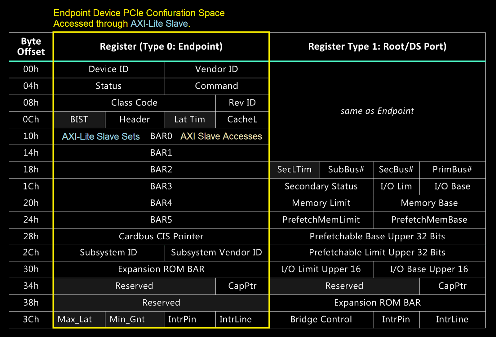


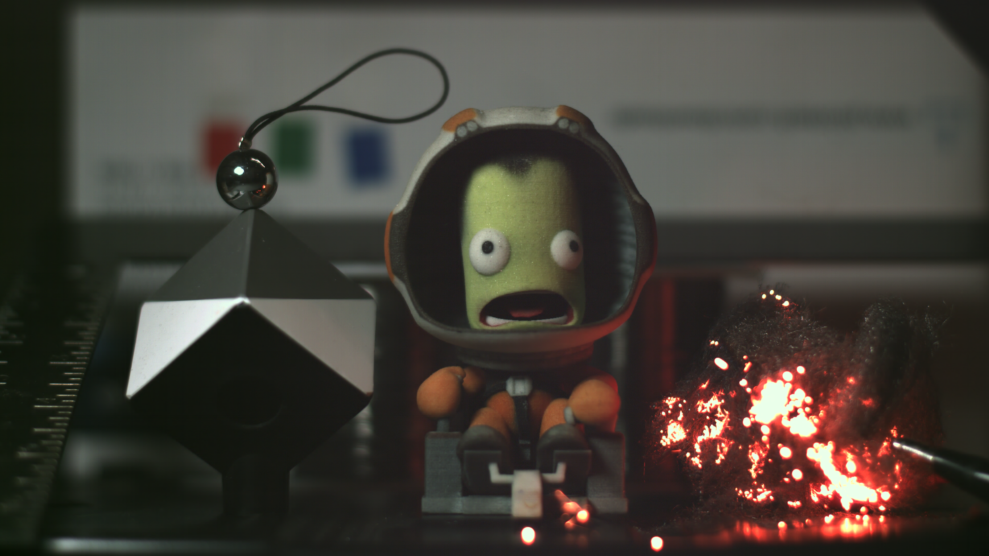